

Manufacturing method of light emitting element
a manufacturing method and light-emitting element technology, applied in the direction of discharge tube/lamp details, discharge tube luminescnet screens, organic semiconductor devices, etc., can solve the problems of inferior heat resistance in comparison with inorganic compounds, improper heat treatment, and low decomposition temperature, so as to reduce the emission brightness over time, enhance the low power consumption of light-emitting elements, and prolong the life.
- Summary
- Abstract
- Description
- Claims
- Application Information
AI Technical Summary
Benefits of technology
Problems solved by technology
Method used
Image

Examples
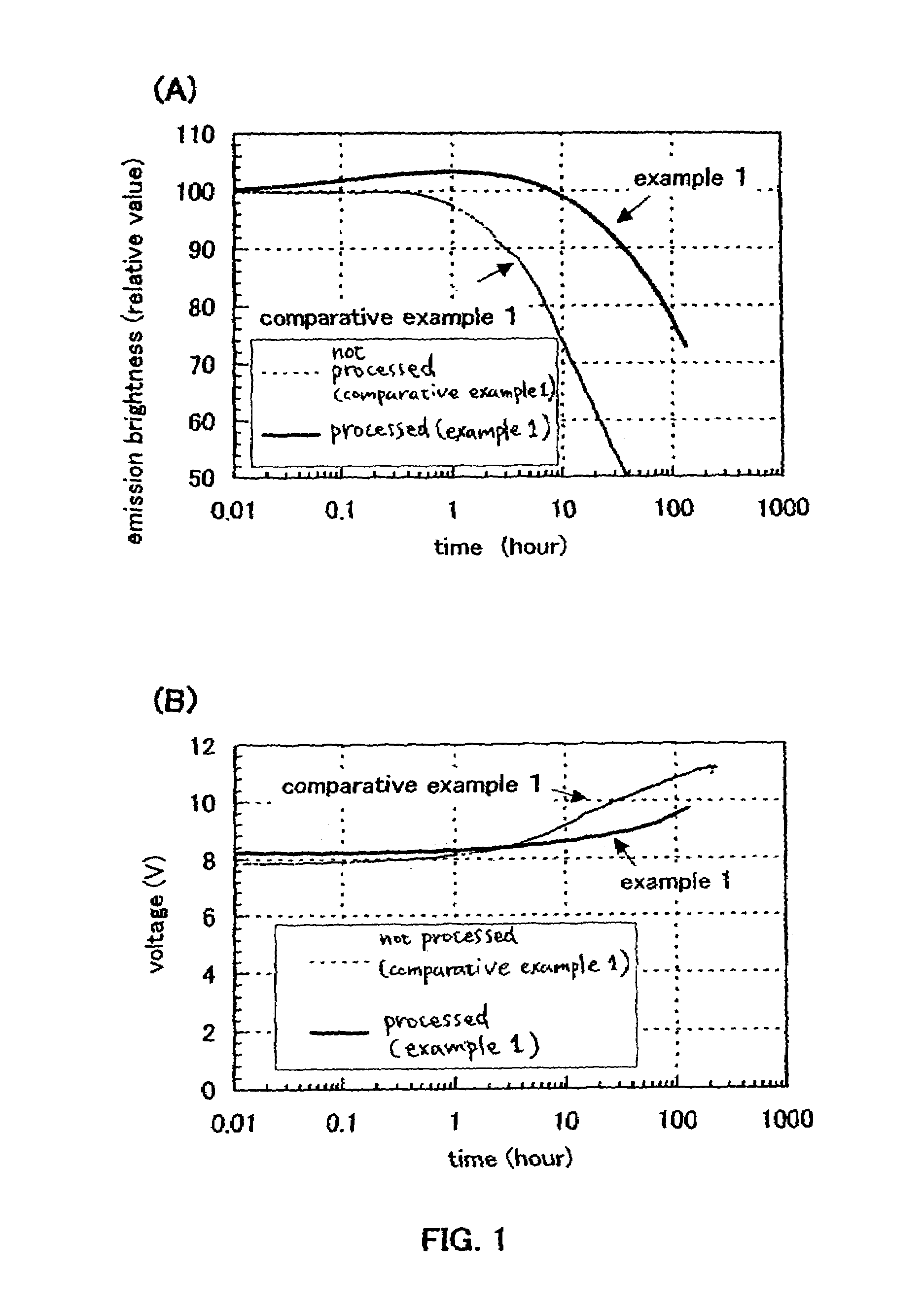
example 1
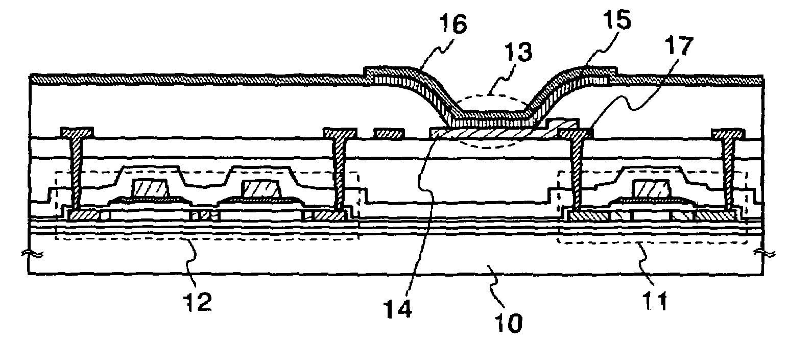
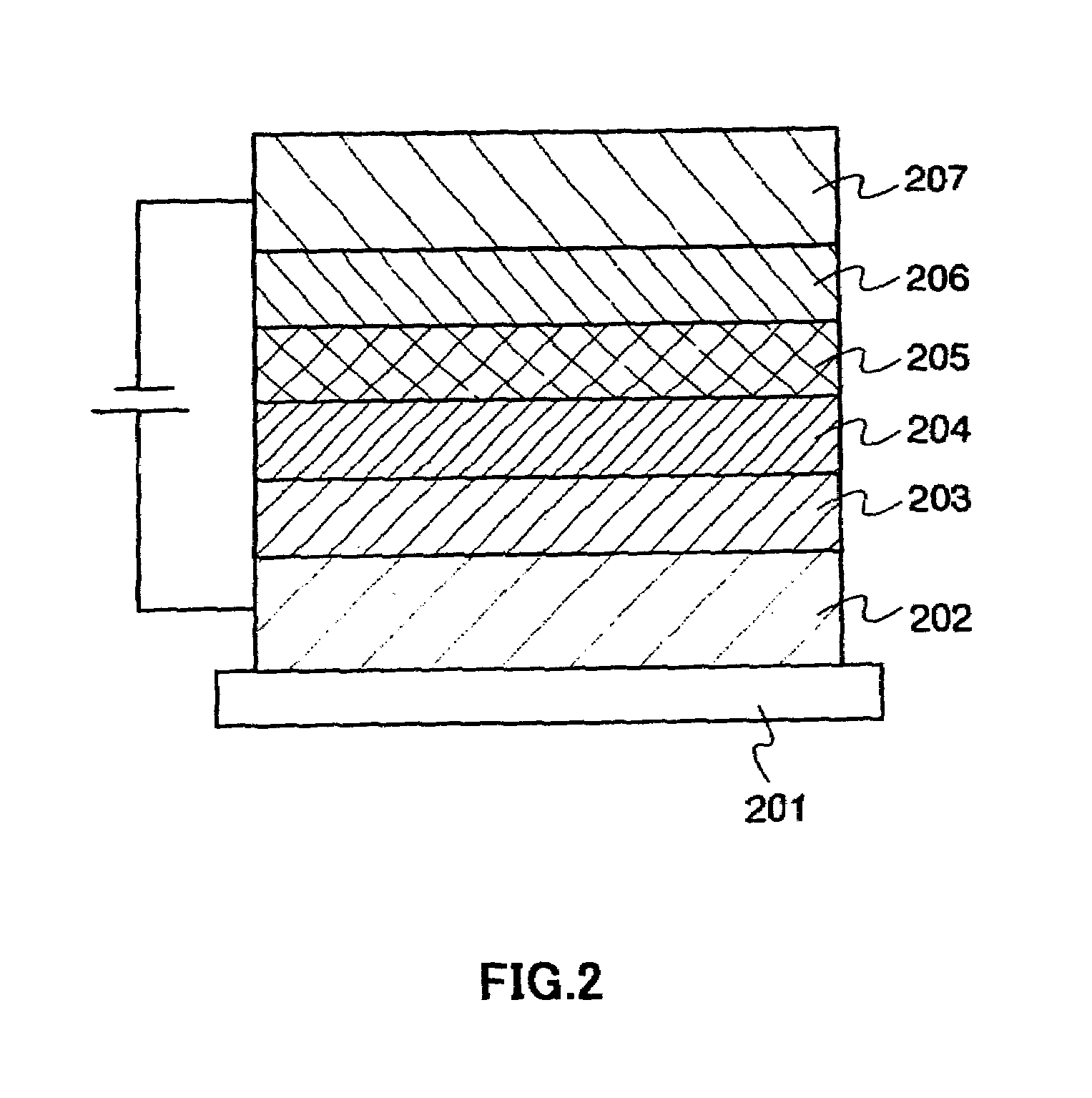
[0043]In this example, a method for manufacturing a light-emitting element shown in FIG. 2 is described. Also, in this example, a light-emitting device manufactured with processing to expose to an atmosphere including oxygen before forming a hole injecting layer is described.
[0044]First, ITO is formed over a substrate 201 by sputtering, thereby forming a first electrode 202.
[0045]Then heat treatment is performed to the substrate 201 over which the ITO is formed at 150° C. for 30 minutes in vacuum kept at 1×10⁻⁵ Pa.
[0046]Next, a substrate 201 to which the process up to forming a first electrode 202 has been performed is exposed to an atmosphere including oxygen. Specifically, 25-sccm oxygen is applied to a treatment chamber in which vacuum degree is kept at 1×10⁻⁵ Pa, and then the substrate 201 is exposed to the chamber in 1.0 Pa and at a room temperature (from 20° C. to 25° C.) for 5 minutes. There is no possibility that the organic compound is decomposed due to the heat since the p...
example 2
[0057]In this example, a light-emitting element shown in FIG. 2 as illustrated in Example 1, which is different in a material for forming a hole injecting layer from the one used in Example 1 is described. In addition, as is the case with Example 1, the light-emitting element is manufactured with processing of exposing to an atmosphere including oxygen before forming the hole injecting layer in this example.
[0058]In this example, a mixture of PEDOT and PSS formed by spin coating is used as a hole injecting layer 203. In addition, as for a first electrode 202; a hole transporting layer 204; a light-emitting layer 205; an electron transporting layer 206; and a second electrode 207, each of the materials, the film thickness, and the formation method is the same as those in Example 1.
[0059]First, ITO is formed over a substrate 201 by sputtering, thereby forming a first electrode 202.
[0060]Next, the substrate 201 over which the ITO is formed is heat treated at 150° C. for 30 minutes in v...
example 3
[0068]In this example, a light-emitting element shown in FIG. 2 as illustrated in Example 1, which is different from Example 1 in the material used for the light-emitting layer is described.
[0069]In this example, a layer formed by co-evaporating DMQd as a guest material with Alq3 is used as a light-emitting layer 205. In addition, while a layer formed by evaporating Alq3 is used as an electron transporting layer 206 as is the case with Example 1, the film thickness thereof is set to 37.5 nm in this Example. As for the first electrode 202, a hole injection layer 203, a hole transporting layer 204, and a second electrode 207, each of the materials, the film thickness, and the formation methods is the same as those in Example 1.
[0070]Further, in this example, three light-emitting elements each of which is the same in the material, the film thickness, and the formation method, but different in the operation part to be exposed to the atmosphere including oxygen are manufactured. The thre...
PUM
 Abstract
Description
Claims
Application Information