Planar lightwave circuit high-speed optical modulator capable of shaping signals

A planar lightwave optical path and optical modulator technology, applied in the field of optoelectronics and integrated optics, can solve the problems of high-speed optical signal wavelength drift, time jitter, burst jitter, etc., to improve wavelength drift, improve performance, and reduce burst jitter Effect

Inactive Publication Date: 2006-12-27
SOUTHEAST UNIV
View PDF0 Cites 0 Cited by
  • Summary
  • Abstract
  • Description
  • Claims
  • Application Information

AI Technical Summary

Problems solved by technology

[0003] No matter what kind of material the planar light wave optical path (PLC) optical modulator is made of, due to factors such as material structure, material growth, process processing, and traveling wave electrode production, some additional effects will be generated under the action of an external high-speed electrical signal, superimposed On the modulated optical signal, it causes wavelength drift, time jitter, burst tremor and other phenomena of high-speed optical signal

Method used


Image

  • Planar lightwave circuit high-speed optical modulator capable of shaping signals
  • Planar lightwave circuit high-speed optical modulator capable of shaping signals
  • Planar lightwave circuit high-speed optical modulator capable of shaping signals

Examples


Embodiment 1

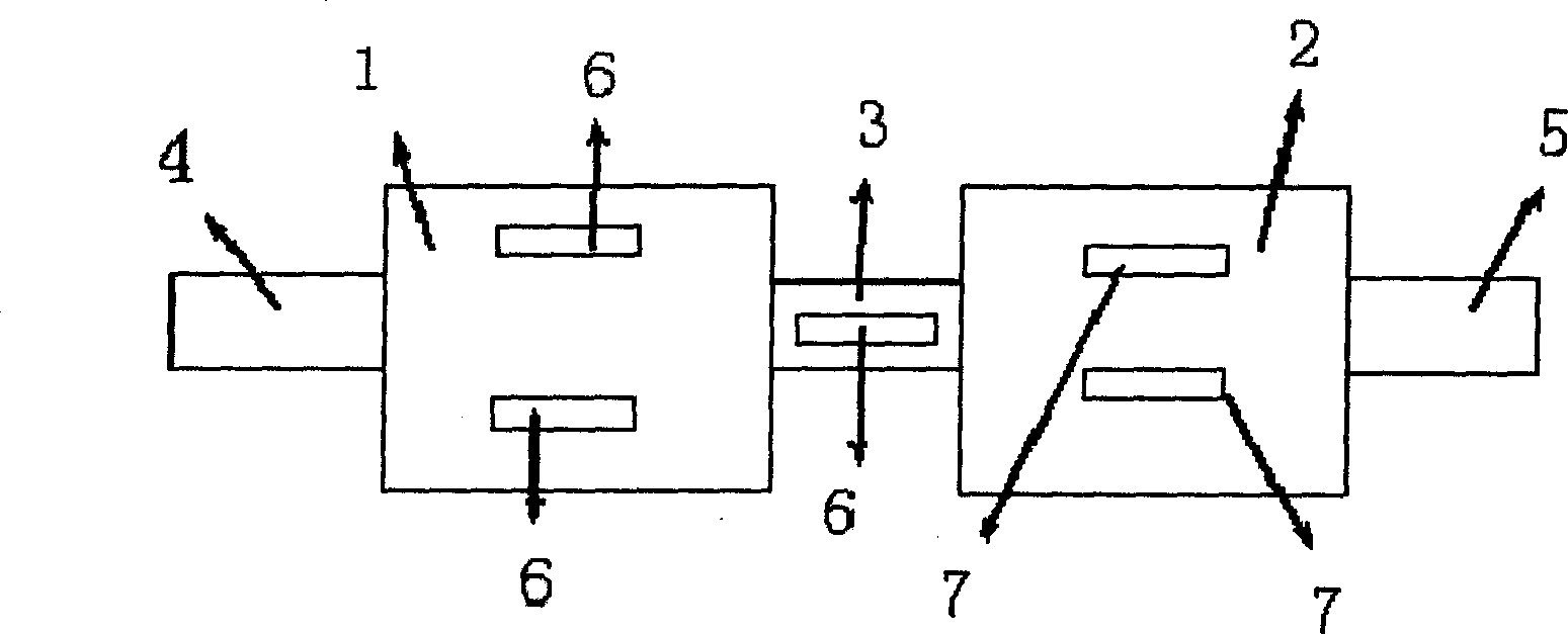
[0024] Figure 4 It is the first example of the present invention, consisting of an input channel 4 , an output channel 5 , a directional coupler 7 , an M-Z type optical modulation module 1 with a shaping component 6 and an adjustable optical shaping module 2 . The light wave is input from the input channel 4 and enters the 3dB directional coupler 7. After being divided by power, it enters the M-Z type optical modulation module 1 in two paths. Under the interaction of the high-speed broadband electrical signal and the material on the traveling wave electrode, the lower optical path The refractive index of the M-Z interferometer is changed, and the light wave at the output of the M-Z interferometer is modulated. At the same time, the shaping element in the M-Z optical modulation module performs preliminary shaping of the optical signal. Then, the optical signal enters the directional coupler again through the intermediate transmission channel, and is adjusted under the action ...

Embodiment 2

[0026] Figure 5 It is the second example of the present invention. It adopts single-port input, output, single-strip optical modulator and single ring resonant cavity modulation structure. Figure 6 is The scanning electron microscope photo of the chip, the terminal of the traveling wave electrode is a matching resistor of 50Ω.

[0027] Figure 7 The electrostatic test results of the optical modulator are given, and the optical signal is tested from Figure 6 Display left input. from Figure 7 (a) It can be seen that since the ring resonant cavity is integrated on the modulator, when there is no external electric field, the room-temperature exciton absorption in the MQW and the resonant cavity produce a common effect, which makes the spectrum sink at 1540nm, and a Filter peak; when the voltage is added to 4.2V ( Figure 7 (b)), the position of the absorption depression moves to the right at 1555nm, and two resonant filter peaks appear at 1535nm and 1565nm; when the volt...


PUM


Abstract

The invention relates to a rectifying plane optical wave light path modulator, which comprises: a light modulating module, a light signal rectifying module, a central transmission channel, an input channel, and an output channel, wherein the invention is characterized in that: the optical wave input and output channels are at two sides of optical modulate module and light signal rectifying module; the controllable modulating light modulating module and controllable modulating light signal rectifying module are both arranged with rectifying elements; the input light via online modulation and rectification of light modulating module and light signal rectifying module is output via output channel. The invention combines the light modulation and signal online instant rectification; uses external control part and rectifying element to reduce the instant fluctuation of high-speed light signal, and compensate the effect caused by wavelength shift and vibration, to form high-quality wideband high-speed light signal.

Description

1. Technical field [0001] The invention belongs to the technical field of optoelectronics and integrated optics, and relates to a planar light wave optical path optical modulator capable of signal shaping, which is used in high-speed optical communication systems, optical computer systems and optical signal processing modules. 2. Background technology [0002] The optical modulator is one of the core components of the dense wavelength division multiplexing (DWDM) optical communication system, and its performance determines the performance of the entire system. For high-speed optical fiber transmission systems, since the direct modulation method of the laser can no longer meet the system requirements, it is an inevitable choice to use an external modulator for optical signal modulation. In this way, the light wave can be modulated at a high speed in a very narrow channel, and at the same time, the chirp generated by the modulator can be used to partially compensate the disper...

Claims


Application Information

Patent Timeline
IPC IPC(8): G02B6/12G02B6/28G02F1/01
Inventor 孙小菡肖金标蔡纯刘旭樊鹤红
Owner SOUTHEAST UNIV
Why Eureka
Try Eureka