Method for eliminating graphic defects of semiconductor wafer edge region

A semiconductor and edge area technology, which is applied in the field of eliminating defect patterns in the edge area of ​​semiconductor wafers, can solve problems such as easy peeling, reduced manufacturing pass rate, short circuit of qualified patterns, etc., to achieve the effect of improving product pass rate and reducing time extension

Inactive Publication Date: 2006-12-27
SEMICON MFG INT (SHANGHAI) CORP +1
View PDF0 Cites 6 Cited by
  • Summary
  • Abstract
  • Description
  • Claims
  • Application Information

AI Technical Summary

Problems solved by technology

When the isolation layer pattern of dynamic random access memory (DRAM) is produced, the rectangular pattern formed at the edge of the semiconductor wafer obviously shrinks, and after the subsequent nitride removal process, the obviously shrunk re...

Method used


Image

  • Method for eliminating graphic defects of semiconductor wafer edge region
  • Method for eliminating graphic defects of semiconductor wafer edge region
  • Method for eliminating graphic defects of semiconductor wafer edge region

Examples


Embodiment Construction

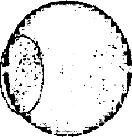
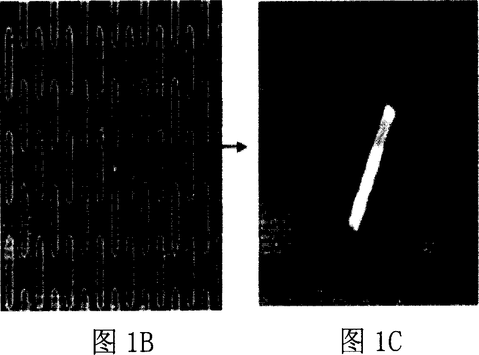
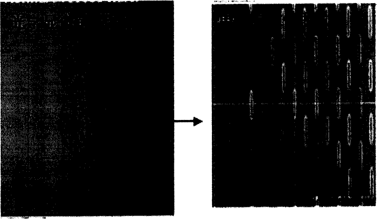
[0031] Taking the active area (Active Area) pattern of a 0.20 μm dynamic random access memory (DRAM) as an example, the method for eliminating pattern defects in the edge area of ​​a semiconductor wafer of the present invention is described.

[0032] The method for eliminating pattern defects in the peripheral regions of semiconductor wafers of the present invention comprises the following process steps:

[0033] 1. Coating photoresist (PR) on the surface of the semiconductor wafer;

[0034] 2. Exposure to photoresist;

[0035] 3. Development;

[0036] 4. Clean the edge area of ​​the semiconductor wafer with a solvent;

[0037] 5. Check;

[0038] 6. Corrosion.

[0039] The new process flow is to add a solvent cleaning step (4) after the step (3) of photoresist development and patterning to remove the abnormal photoresist shrinkage and deformation pattern on the edge of the semiconductor wafer.

[0040] New process flow: coating photoresist→exposing photoresist→developing→...


PUM


Abstract

The invention relates to a method for eliminating the image defect at the edge area of semi-conductor crystal chip, which is characterized in that: the invention adds the process that washing the edge of chip after the developing process that forming optical etching image; and eliminates the constriction deformation image in the edge area, to avoid the constriction deformation image being removed to cause defects on other qualified images of chip, to improve the pass percentage of product.

Description

technical field [0001] The invention relates to a method for eliminating defect patterns in the edge region of a semiconductor wafer. Background technique [0002] In the manufacture of semiconductor devices, the current common basic process flow for forming photoresist (PR) patterns is: coating photoresist on the surface of the semiconductor wafer→exposing the photoresist→developing→etching. Due to the limitations and defects of currently used photolithography equipment and photolithography process, the pattern in the edge region of the semiconductor wafer produced by this general manufacturing method is deformed, or the pattern size is abnormal. During the subsequent process of manufacturing semiconductor devices, the abnormally sized deformed patterns in the edge region of the semiconductor wafer will be peeled off, and the debris of the peeled patterns will fall on the normal patterns on the semiconductor wafer, damaging the normal patterns. Therefore, the peeling of de...

Claims


Application Information

Patent Timeline
IPC IPC(8): G03F7/00G03F7/42
Inventor 陈自凡蔡奇澄姚欣林爱钦庄晓辉
Owner SEMICON MFG INT (SHANGHAI) CORP
Why Eureka
Try Eureka