
High-brightness light emitting diode having reflective layer

A technology of light-emitting diodes and light-emitting structures, applied in electrical components, circuits, semiconductor devices, etc., can solve the problems of weak chip bonding force, redistribution, and rough reflective surface.

Inactive Publication Date: 2007-01-17
VISUAL PHOTONICS EPITAXY
View PDF4 Cites 10 Cited by
  • Summary
  • Abstract
  • Description
  • Claims
  • Application Information

AI Technical Summary

Problems solved by technology

However, the problem with the use of a transparent substrate in the first method is that the die attach must be carried out at a high tempering temperature for a period of time, which will cause the redistribution of dopants in it, thereby reducing the efficiency of the LED
The problem with the use of mirrors in the second method is that the reflective surface of the mirror is directly used for bonding during the die bonding process, so the reflective surface will be rough or deteriorated, and the reflective surface of the mirror will be polluted
If the alloy metal layer is too thin, the ohmic contact between the alloy metal and the light-emitting structure will be poor, but if the alloy metal layer is too thick, the bonding force after chip bonding will be weak

Method used


Image

  • High-brightness light emitting diode having reflective layer
  • High-brightness light emitting diode having reflective layer
  • High-brightness light emitting diode having reflective layer

Examples


Embodiment Construction

[0041] The following description is only used as an example, but not intended to limit the scope, application or configuration of the present invention. Since the following descriptions are only examples of implementing the present invention, various functions and configuration modifications and changes can be made to the components of these examples without departing from the spirit and scope of the present invention, and all of them are included in the scope of the claims and its scope. Among the equals.

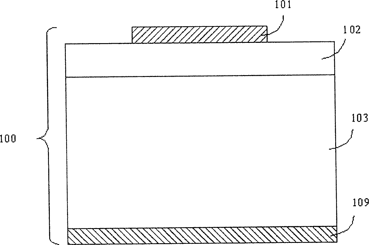
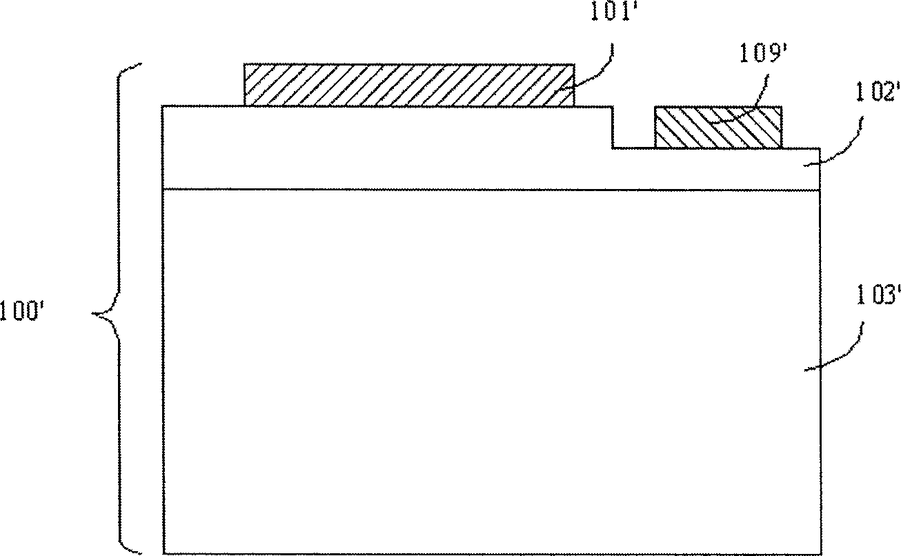
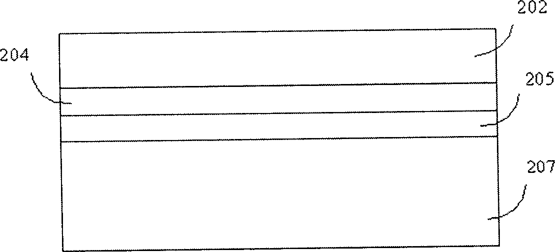
[0042] Figure 2a is a schematic cross-sectional view of a light emitting diode structure according to an embodiment of the present invention. like Figure 2a As shown, the light emitting structure 202 includes a light emitting structure 202 . The light emitting structure 202 includes a p-n junction active layer, which can emit light due to conducting current. The light emitting structure 202 generally includes, but is not limited to, multiple layers of III-V compound ...


PUM


Abstract

An LED structure is disclosed herein, which comprises, sequentially arranged in the following order, a light generating structure, a non-alloy ohmic contact layer, a metallic layer, and a substrate. As a reflecting mirror, the metallic layer is made of a pure metal or a metal nitride for achieving superior reflectivity. The non-alloy ohmic contact layer is interposed between the metallic layer and the light generating structure so as to achieve the required ohmic contact. To prevent the metallic layer from intermixing with the non-alloy ohmic contact layer and to maintain the flatness of the reflective surface of the first metallic layer, an optional dielectric layer is interposed between the metallic layer and the non-alloy ohmic contact layer.

Description

technical field [0001] The present invention relates to a light emitting diode, and more particularly, the present invention relates to a light emitting diode with a reflective layer to solve the light absorption problem of the light emitting diode substrate. Background technique [0002] Figure 1a is a schematic cross-sectional view of a known light-emitting diode structure. like Figure 1a As shown, the light emitting diode 100 includes: a semiconductor substrate 103; a light emitting structure 102, which is located on the semiconductor substrate 103; . [0003] The light-emitting structure 102 is generally composed of multiple layers of Al-containing III-V compound semiconductor layers, such as AlGaAs that emits infrared light and red light, or AlGaInP that emits yellow-green, yellow, and red light. The material of the substrate 103 is usually gallium arsenide (GaAs), and the lattice constant of GaAs can match the lattice constant of the light emitting structure 102 . ...

Claims


Application Information

Patent Timeline
Patent Type & Authority Applications(China)
IPC IPC(8): H01L33/00H01L33/38H01L33/40
CPCH01L33/0079H01L33/387H01L33/405H01L33/0093
Inventor 王会恒刘进祥林昆泉
Owner VISUAL PHOTONICS EPITAXY
Learn More