Field effect transistor and application device thereof

A field effect transistor, conductive type technology, applied in the field of field effect transistors and their application devices, can solve problems such as unpredictable

Inactive Publication Date: 2007-01-24
KK TOSHIBA
View PDF1 Cites 10 Cited by
  • Summary
  • Abstract
  • Description
  • Claims
  • Application Information

AI Technical Summary

Problems solved by technology

However, in this configuration, the withstand voltage of the device is designed to be below several hundred volts, resulting in the same disadvantages as the above-mentioned horizontal device,

Method used


Image

  • Field effect transistor and application device thereof
  • Field effect transistor and application device thereof
  • Field effect transistor and application device thereof

Examples


Embodiment 1

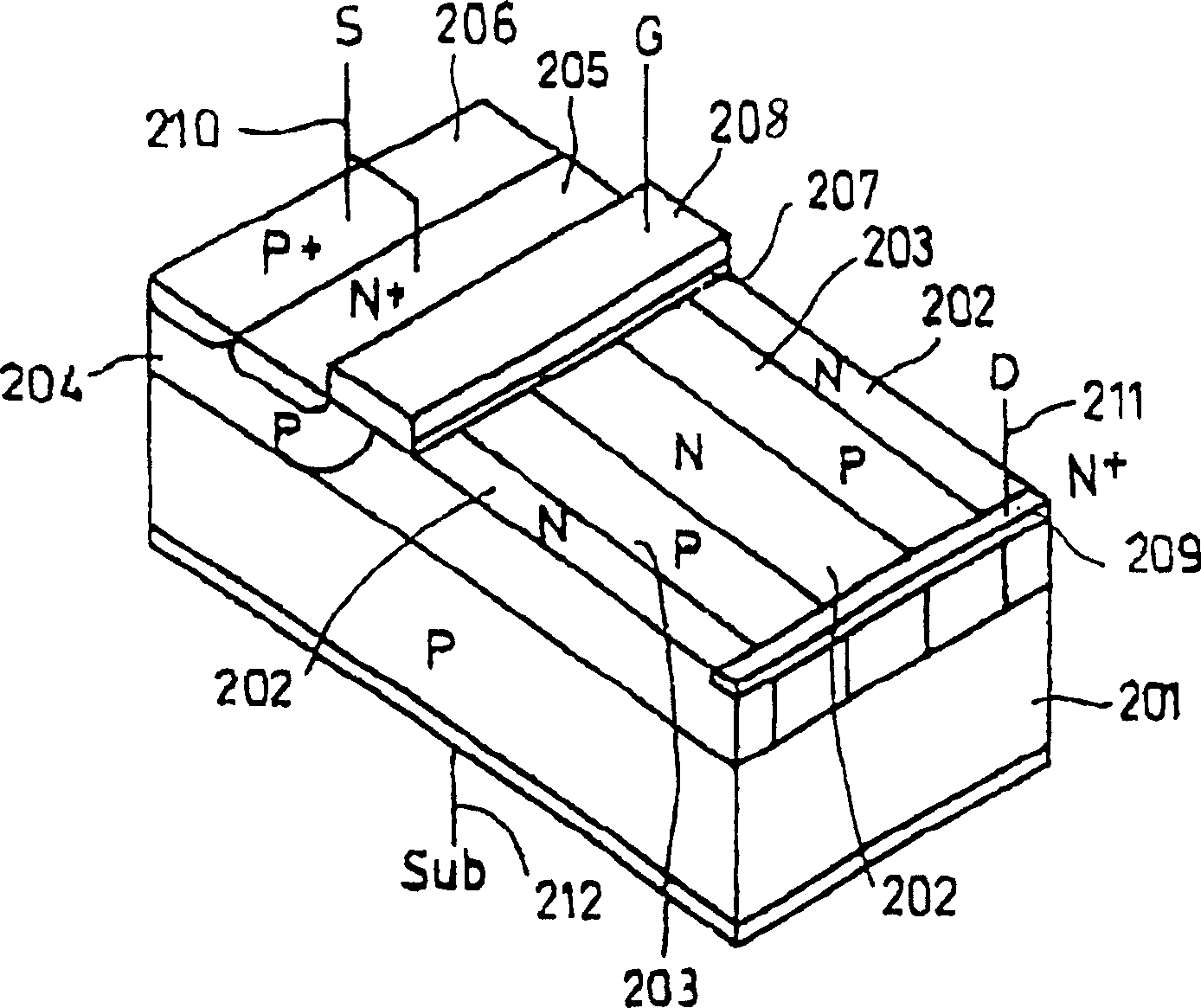
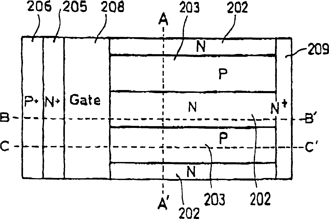
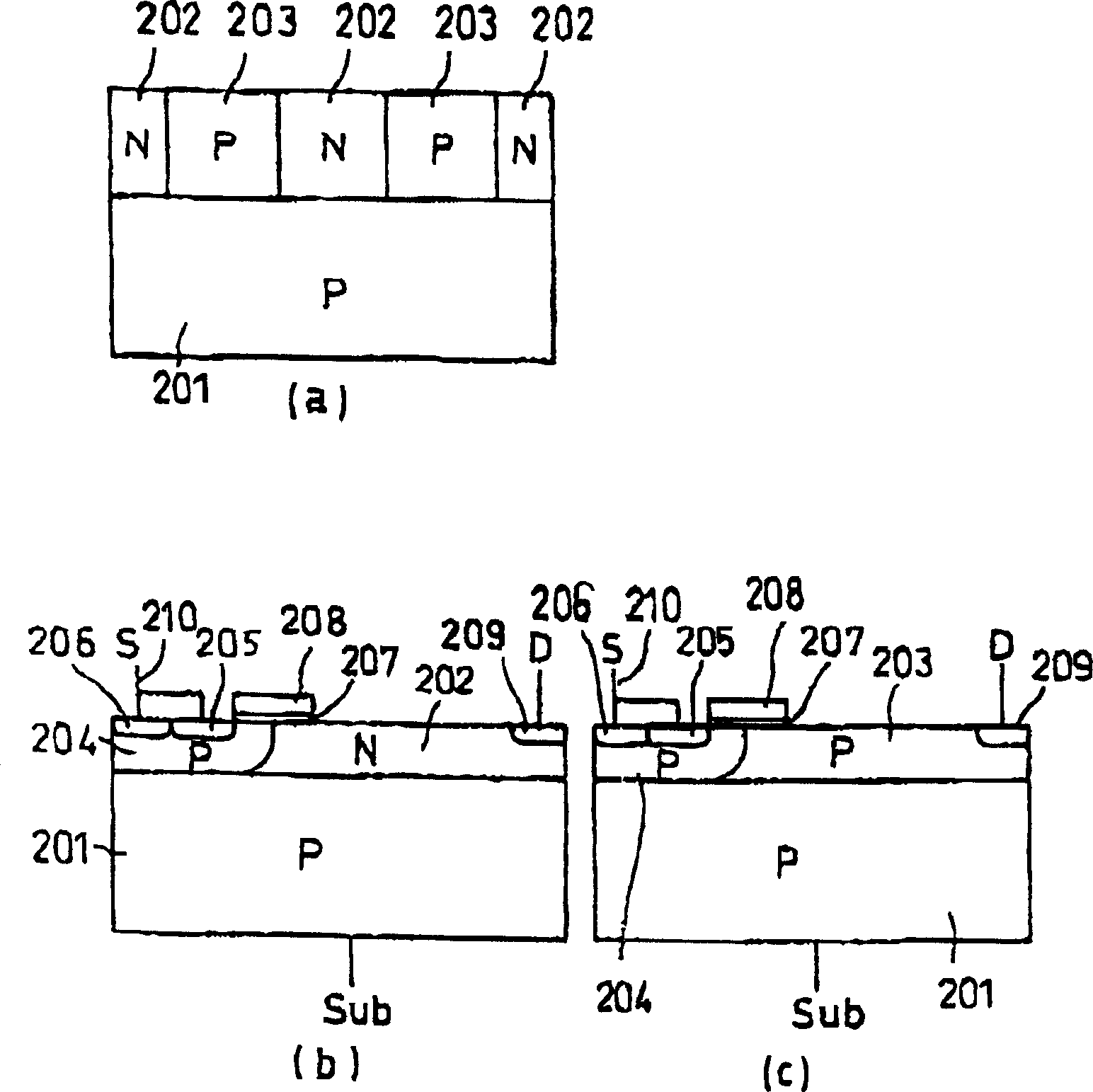
[0052] Figure 4 to Figure 7 This is Example 1 of the present invention, and is a diagram showing the structure of a lateral field effect transistor (hereinafter, the field effect transistor is simply referred to as MOSFET). Figure 4 , Fig. 5 is its three-dimensional oblique view, and Fig. 6 is its top view, Figure 7 (a) to (d) are respectively along image 3 The A-A', B-B', C-C' lines cut the cross-sectional view of the device. and, Figure 4 It is a perspective view showing part of the device shown in FIG. 5 excluding it. The horizontal MOSFET is a so-called MOSFET called a multi-resurf MOSFET or a super-junction MOSFET.

[0053] As shown in the figure, a substrate 1 is composed of a p-type (or n-type) silicon semiconductor 2 and a buried oxide film 3 stacked on its surface. On the buried oxide film 3, a p-type base layer 4 is selectively formed. On top of p-type base layer 4, high-concentration n-type source layer 5 and high-concentration p-type contact layer 6 are ...

Embodiment 2

[0068] Figure 15 to Figure 18 This is Example 2 of the present invention, and is a diagram showing the structure of a lateral MOSFET. Figure 15 is its oblique view, Figure 16 is its top view, Figure 17 , Figure 18 are along Figure 16 The cross-sectional view of the A-A', B-B' line of the device.

[0069] In this embodiment, the active layer formed by the p-type base layer 4, the n-type drain layer 7, the n-type drift semiconductor layer 12 and the p-type drift semiconductor layer 13 formed between them, is formed on the SOI insulating substrate The bottom 1 is formed in a columnar shape. In addition, it is a structure in which both sides of the columnar active layer are sandwiched by gate electrodes 15 . In addition, in the active layer sandwiched by the gate electrodes 15, n-type drift semiconductor layers 12 and p-type drift semiconductor layers 13 of a superstructure structure are alternately stacked. In these figures, with Figure 4 The same parts as in FIG. ...

Embodiment 3

[0072] Figure 20 to Figure 23 It is a perspective perspective view showing the structure of a vertical trench gate MOSFET according to Embodiment 3 of the present invention.

[0073] Figure 21 It is a perspective view in which the vertical MOSFET shown in FIG. 20 is cut longitudinally and shows half thereof. As can be seen from these figures, in this embodiment, relative to Figure 15 The vertical MOSFET shown is different in that the gate electrode has a groove structure, and the n-type drift semiconductor layer 12 and the p-type drift semiconductor layer 13 are extended vertically and arranged horizontally.

[0074] in addition, Figure 22 is showing Figure 21 change example. As shown in the figure, although the n-type drift semiconductor layer 12 and the p-type drift semiconductor layer 13 are extended vertically, they are different in that they are stacked alternately from one of the two gate electrodes 15, 15' to the other. .

[0075] Again, if Figure 23 The v...


PUM

PropertyMeasurementUnit
Thicknessaaaaaaaaaa
Thicknessaaaaaaaaaa
Thicknessaaaaaaaaaa

Abstract

The present invention provides a MOSFET having a low on-state resistance and a high withstand voltage as well as a small output capacitance (C(gd), etc.). The MOSFET has a p-type base layer and a n-type source layer selectively formed on the surface of the p-type base layer. A n-type drain layer is formed in a position apart from the p-type base layer . On the surface of the region between the p-type base layer and the n-type drain layer, a n-type drift semiconductor layer and a p-type drift semiconductor layer are alternately arranged from the p-type base layer 4 to the n-type drain layer. Further, in the region between the n-type source layer and the n-type drain layer, a gate electrode is formed via a gate insulating film. With the structure, the neighboring region of the gate electrode is depleted by a built in potential between the n-type drift semiconductor layer and the p-type drift semiconductor layer or by the potential of the gate electrode, when the gate electrode, source electrode, and drain electrode are at 0 potential.

Description

[0001] This application is a divisional application of the Chinese patent application No. 03107543.6 filed on March 27, 2003 with the title of "Field Effect Transistor and Its Applied Devices". technical field [0002] The invention relates to a field effect transistor, in particular to a field effect transistor with low conduction resistance and small output capacitance and an application device thereof. Background technique [0003] Figure 1 to Figure 3 It is a multi RESURF (REduced SURface Field) MOSFET that is an existing low on-resistance horizontal field effect transistor (hereinafter referred to as a MOSFET for short). In addition, the structure of a MOSFET called a superjunction structure is shown in the figure , figure 1 is its oblique view, figure 2 is its top view, image 3 (a), (b), (c) are along the figure 2 The lines A-A', B-B', and C-C' respectively cut the cross-sectional view of the device. [0004] As shown in these figures, a p-type base layer 204 ...

Claims


Application Information

Patent Timeline
IPC IPC(8): H01L29/78H03K17/78
CPCH01L29/7824H01L29/0634H01L29/0878H01L29/1095H01L29/7831
Inventor 北川光彦相泽吉昭
Owner KK TOSHIBA
Why Eureka
Try Eureka