DMOSFET and planar type MOSFET

A planar and N-type technology, applied in diodes, semiconductor devices, electrical components, etc., can solve the problems of reducing on-resistance, channel layer punch-through, and withstand voltage drop, achieving reduced loss, low feedback capacitance, low Effect of on-resistance

Inactive Publication Date: 2007-02-28
RENESAS TECH CORP
View PDF1 Cites 13 Cited by
  • Summary
  • Abstract
  • Description
  • Claims
  • Application Information

AI Technical Summary

Problems solved by technology

[0010] However, in the above-mentioned planar MOSFET of Patent Document 1, the miniaturization of the cell size is insufficient, and the on-resistance is still high compared with the trench MOSFET, so it is necessary to study how to further reduce the on-resistance
In addition, in planar MOSFETs, it is known that shallow junctions in the channel layer are sufficient in order to reduce on-resistance without being affected by JFET resistance components. The depth is about 0.8μm, and the research on the shallow junction is insufficient
In addition, since the dispersion of the channel in the lateral direction is also reduced if the channel layer is made shallower, there are problems in the structure of the planar MOSFET that the channel layer penetrates and the withstand voltage drops.
Therefore, no research has been conducted on planar MOSFETs having shallow channel layers such as channel depths of 0.5 μm or less

Method used


Image

  • DMOSFET and planar type MOSFET
  • DMOSFET and planar type MOSFET
  • DMOSFET and planar type MOSFET

Examples


Embodiment Construction

[0046] Hereinafter, embodiments of the present invention will be described in detail with reference to the drawings. In addition, in all the drawings for explaining the embodiment, as a matter of principle, the same reference numerals are given to the same members, and overlapping description thereof will be omitted.

[0047] (Embodiment 1)

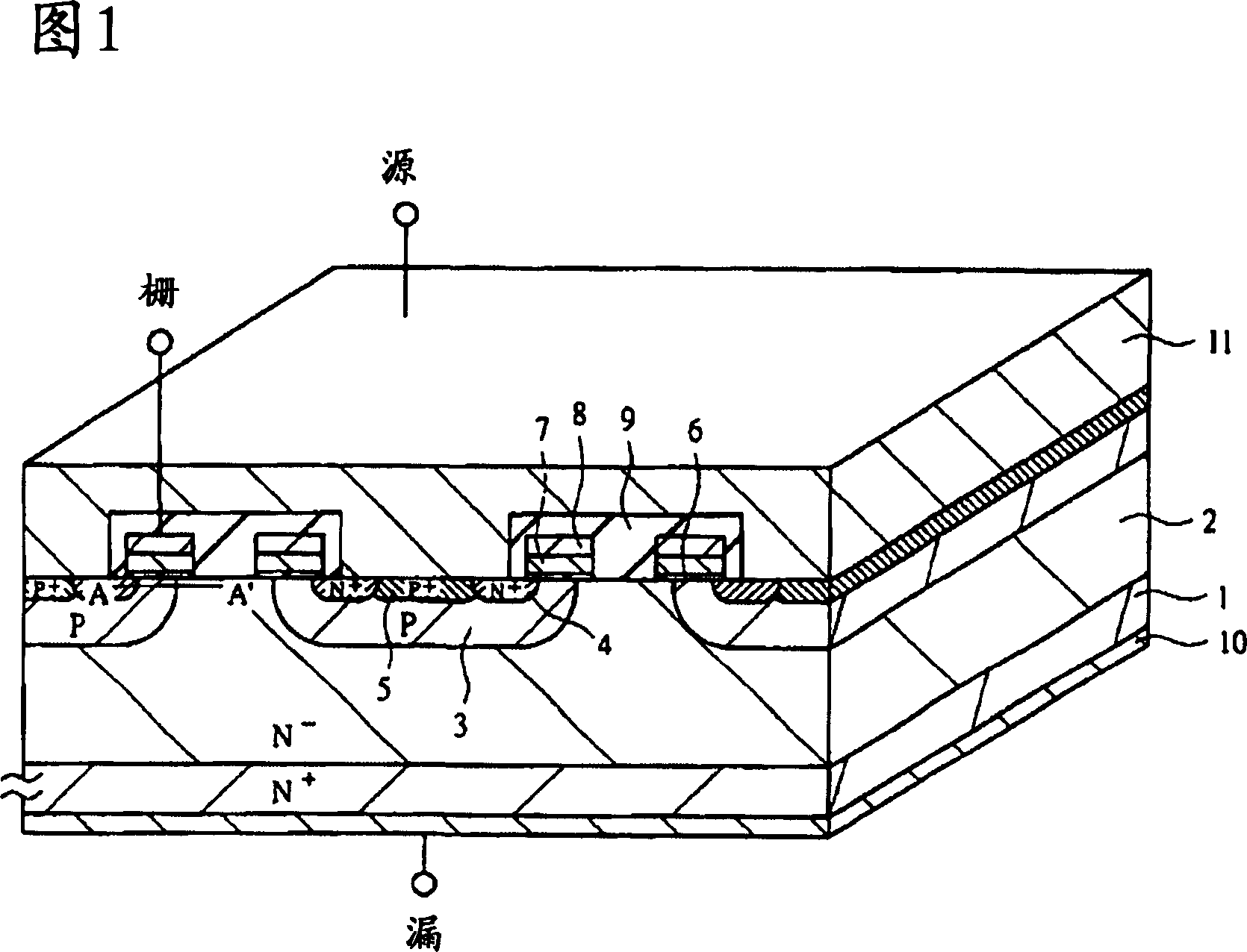
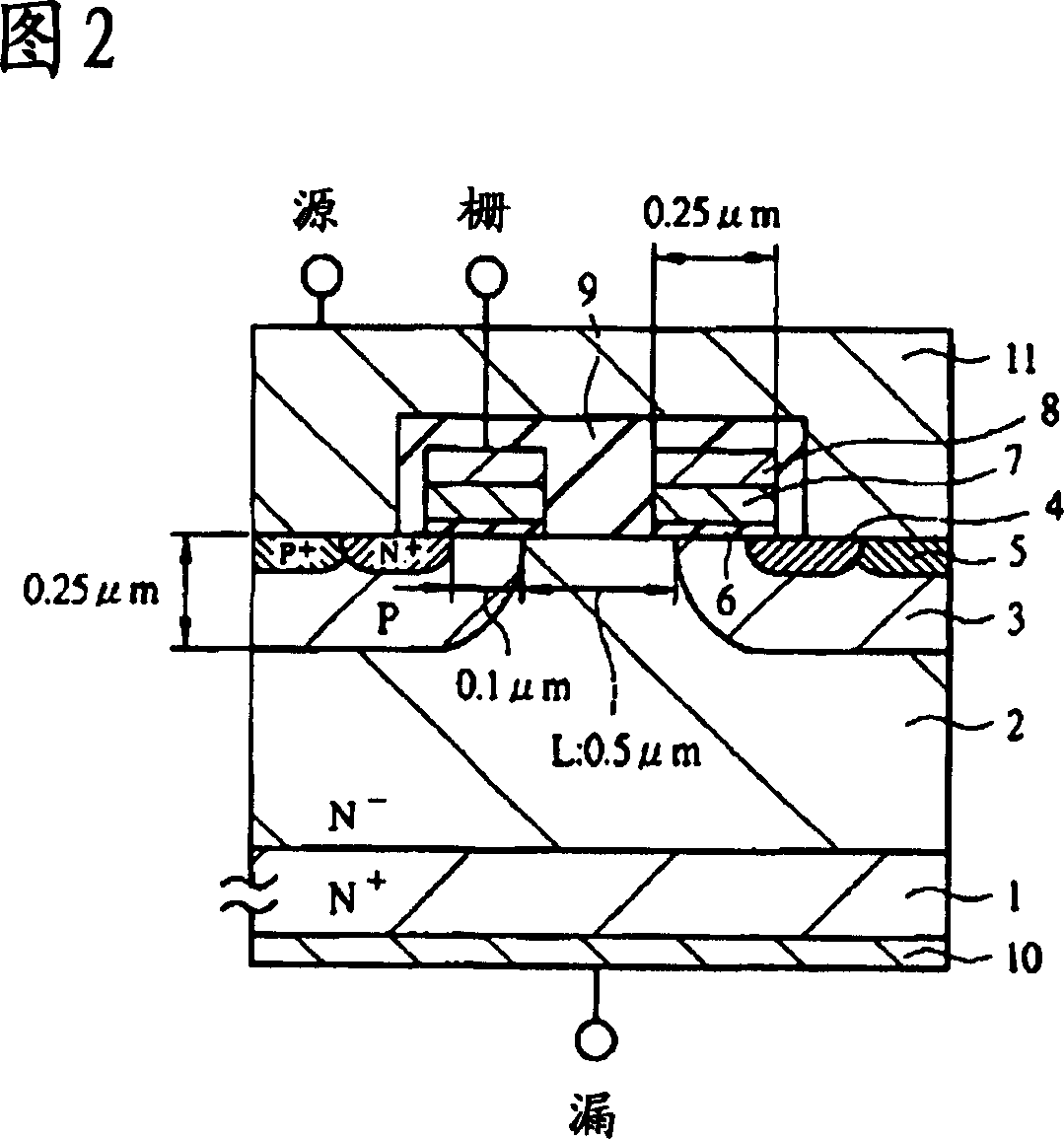
[0048] Embodiment 1 of the present invention will be described using FIGS. 1 to 8 . Fig. 1 shows a cross-sectional structure of a planar MOSFET according to Embodiment 1 of the present invention. Fig. 2 shows an example of dimensions of the planar MOSFET according to Embodiment 1 of the present invention.

[0049]The planar MOSFET of the present embodiment 1, as shown in FIG. 1, is a planar N-channel DMOSFET (double-diffused MOSFET). + N on substrate 1 - epitaxial layer 2, in which the N - P-type channel layer 3, N + The source region 4 and the body contact region 5 form the P-type polysilicon 7 of the gate electrode through the gat...


PUM


Abstract

A technology capable of realizing a MOSFET with low ON-resistance and low feedback capacitance, in which the punch through of a channel layer can be prevented even when the shallow junction of the channel layer is formed in a planar type MOSFET is provided. A P type polysilicon 7 is used for a gate electrode in a planar type MOSFET, in particular, in an N channel DMOSFET.

Description

technical field [0001] The present invention relates to a power MOSFET (Metal Oxide Semiconductor-Field Effect Transistor), in particular to a structure suitable for realizing low on-resistance and low feedback capacitance in a low withstand voltage power MOSFET with a withstand voltage of about 100V or less and its manufacture The method further relates to a technology applicable and effective in a power supply device using the power MOSFET. Background technique [0002] For example, non-isolated DC / DC converters used in power supply devices such as desktop PCs, notebook PCs, and game consoles are accompanied by increased current and As a passive component, choke coils and input and output capacitors are required to be miniaturized, etc., and there is a trend of higher current and higher frequency. The above-mentioned DC / DC converter is composed of a high-side switch and a low-side switch, and power MOSFETs are used in each of these switches. [0003] These switches perfo...

Claims


Application Information

Patent Timeline
Patent Type & Authority Applications(China)
IPC IPC(8): H01L29/78H01L29/49H01L29/36
CPCH01L29/4916H01L29/0878H01L29/66712H01L29/402H01L29/086H01L29/7802H01L29/42372H01L29/0634H01L29/42368H01L29/518H01L29/1095H01L29/0696H01L29/7806H01L29/4933
Inventor 白石正树岩崎贵之松浦伸悌中沢芳人可知刚
Owner RENESAS TECH CORP
Why Eureka
Try Eureka