Photomultiplier

An electron multiplier and optoelectronic technology, which is applied to electron multiplier tubes, electron multiplier anode devices, electron multiplier detailed information, etc. and other problems, to achieve the effect of increasing the doubling efficiency

Active Publication Date: 2007-02-28
HAMAMATSU PHOTONICS KK
View PDF1 Cites 0 Cited by
  • Summary
  • Abstract
  • Description
  • Claims
  • Application Information

AI Technical Summary

Problems solved by technology

In particular, the finer the parts themselves, the more difficult it is to realize the precise arrangement of the parts, and it is impossible to

Method used


Image

  • Photomultiplier
  • Photomultiplier
  • Photomultiplier

Examples


Embodiment Construction

[0036] Next, the photoelectron multiplier of the present invention and its manufacturing method will be described in detail with reference to FIGS. 1 to 10 . In addition, in the description of the drawings, the same symbols are used for the same parts, and repeated descriptions are omitted.

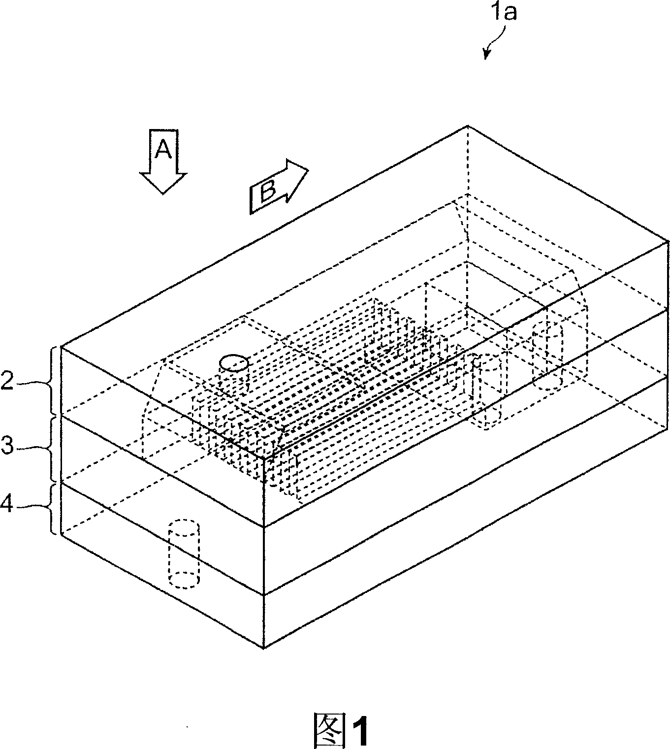
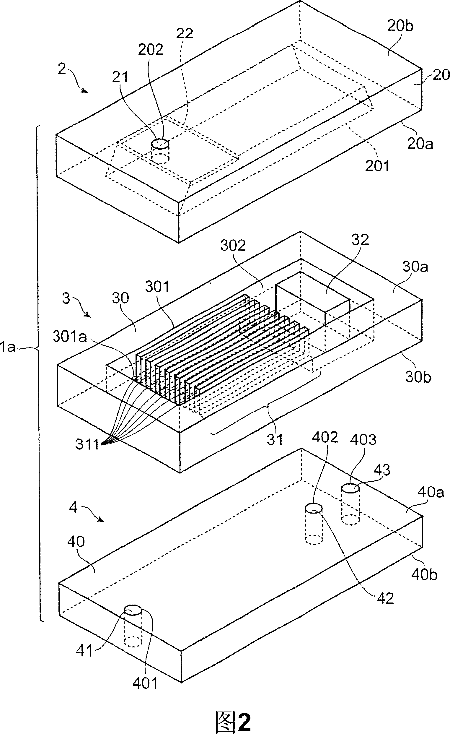
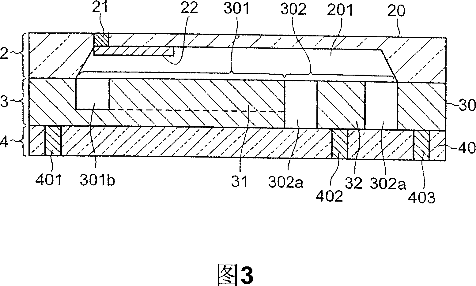
[0037] FIG. 1 shows a perspective view of the structure of an embodiment of the photoelectron multiplier of the present invention. The photoelectron multiplier 1a shown in FIG. 1 is a transmissive electron multiplier, comprising an upper frame 2 (glass substrate), a side wall frame 3 (silicon substrate), and a lower frame 4 (glass substrate). peripheral device. In this photoelectron multiplier 1a, the traveling direction of the electrons in the electron multiplier part intersects the incident direction of light toward the photoelectric surface, that is, after the light is incident from the direction indicated by arrow A in FIG. 1, the photoelectrons emitted from the photoelectric surface...


PUM


Abstract

The invention relates to a photoelectron multiplier with a fine structure realizing high multiplication efficiency. The photoelectron multiplier includes a peripheral device that maintains a vacuum inside, and in the peripheral device, a photoelectric surface that emits photoelectrons corresponding to incident light is arranged, and an electron multiplication unit that cascades and multiplies the photoelectrons emitted from the photoelectric surface is used to extract the photoelectron generated by the photoelectron multiplier. The anode for the secondary electrons generated by the electron multiplier. In particular, in the electron multiplier part, a groove part for cascade multiplication of photoelectrons from the photoelectric surface is formed, and on each surface of a pair of wall parts (311) defining the groove part, a secondary electron is formed on the surface. One or more protrusions (311a) on the emission surface.

Description

technical field [0001] The present invention relates to a photoelectron multiplier having an electron multiplier that multiplies a cascade of photoelectrons generated by a photosurface. Background technique [0002] Conventionally, a photoelectron multiplier (PMT: Photo-Multiplier Tube) has been known as a photosensitive element. A photoelectron multiplier includes a photocathode for converting light into electrons, a focusing electrode, an electron multiplier, and an anode, and houses them in a vacuum container. In the photoelectron multiplier, when light is incident on the photoelectric surface, photoelectrons are released from the photoelectric surface in the vacuum container. The photoelectrons are guided into the electron multiplication part by the focusing electrode, and cascaded and multiplied by the electron multiplication part. The anode outputs arriving electrons among the multiplied electrons as a signal (for example, refer to the following Japanese Patent Docum...

Claims


Application Information

Patent Timeline
IPC IPC(8): H01J43/24H01J43/12H01J43/28
CPCH01J43/24H01J43/04H01J9/26H01J43/08
Inventor 久嵨浩之下井英树影山明广井上圭祐伊藤益保
Owner HAMAMATSU PHOTONICS KK
Why Eureka
Try Eureka