Method for improving voltage distribution of component threshold value

A threshold voltage distribution and device technology, applied in semiconductor/solid-state device manufacturing, circuits, electrical components, etc., can solve the problems of threshold voltage distribution device characteristic drift, poor device stability, etc., to reduce LDD atomic diffusion, reduce leakage current, Effect of Uniform Threshold Voltage Distribution

Active Publication Date: 2007-03-14
SHANGHAI HUAHONG GRACE SEMICON MFG CORP
View PDF0 Cites 7 Cited by
  • Summary
  • Abstract
  • Description
  • Claims
  • Application Information

AI Technical Summary

Problems solved by technology

Uneven threshold voltage distribution can easily lead to device characteristic drift caused by process fluctuations, and the stability of the device is poor

Method used


Image

  • Method for improving voltage distribution of component threshold value
  • Method for improving voltage distribution of component threshold value
  • Method for improving voltage distribution of component threshold value

Examples


Embodiment Construction

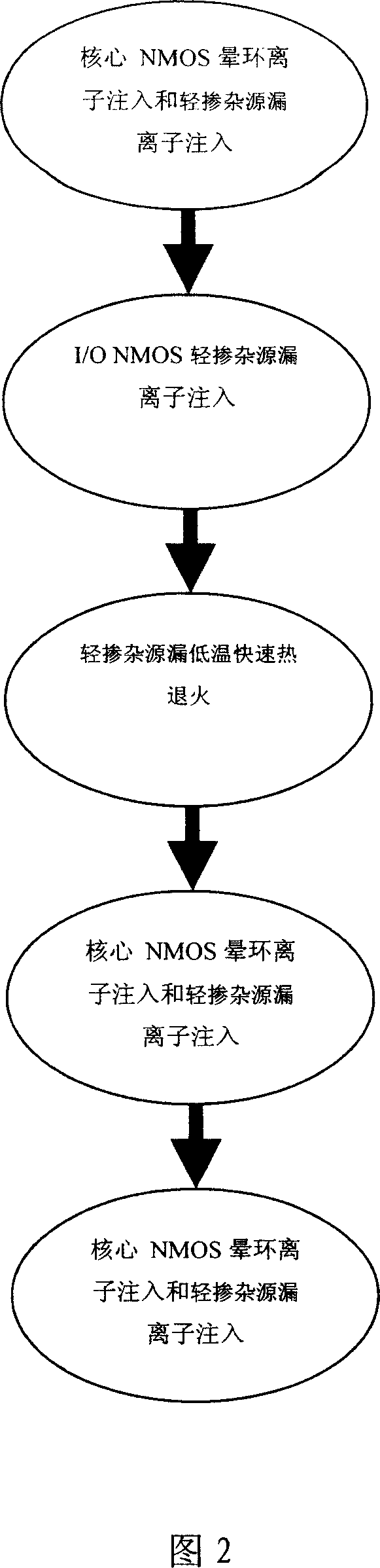
[0013] As shown in Figure 2, a kind of method step of improving device threshold voltage distribution of the present invention is: at first, carry out core NMOS halo ion implantation and LDD ion implantation; Second step, I / O NMOS LDD ion implantation; Third step, LDD low temperature rapid thermal annealing; the fourth step, core PMOS halo ion implantation and LDD ion implantation; fifth step, I / O PMOS LDD ion implantation. The conditions of the LDD low-temperature rapid thermal annealing in the third step may be that the temperature is 950° C., and the low-temperature rapid thermal annealing time is 10 seconds.

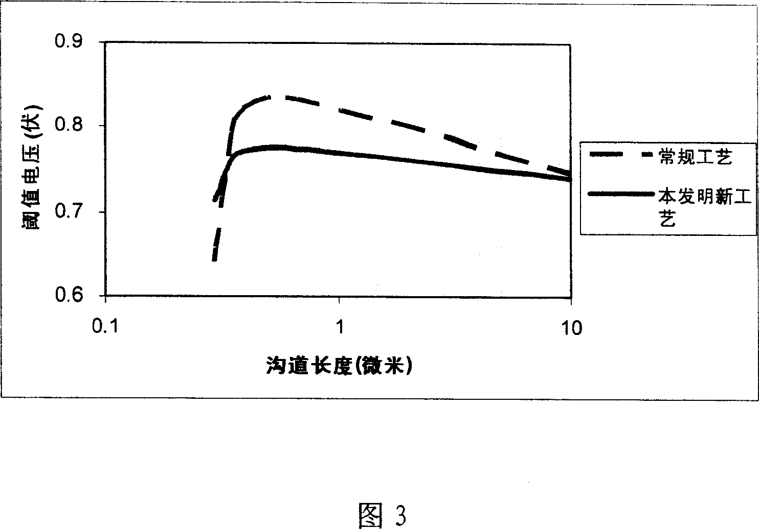
[0014] The invention discloses a method for improving the threshold voltage distribution of devices, which adopts low-temperature rapid thermal annealing after I / O NMOS LDD ion implantation to eliminate lattice defects, eliminate interstitial atoms and vacancies, and reduce boron and phosphorus atoms caused by lattice defects The enhanced diffusion can effectively re...


PUM


Abstract

This invention discloses one method to improve parts valve voltage distribution, which comprises the following steps: core NMOS air ring ion injection and LDD ion injection; I/O NMOS and LDD ion injecting; c, LDD low temperature rapid annealing; d, core PMOS air ring ion injecting and LDD ion injecting; e, I/O PMOS LDD ion injecting.

Description

technical field [0001] The invention relates to a semiconductor device and a semiconductor manufacturing process, in particular to a method for improving device threshold voltage distribution in NMOS device manufacturing. Background technique [0002] Short Channel Effect (SCE) and Reverse Short Channel Effect (RSCE) are two important effects that exist in NMOS devices at the same time, and they will cause the threshold voltage of NMOS devices There is a large fluctuation with the change of the channel length. RSCE causes the threshold voltage of NMOS devices to increase with the decrease of the channel length within a certain channel length range, and SCE causes the short channel threshold voltage to decrease. The uneven distribution of the threshold voltage will easily lead to device characteristic drift caused by process fluctuations, and the stability of the device is poor. Especially for input / output (input / output, hereinafter referred to as I / O) NMOS devices, because...

Claims


Application Information

Patent Timeline
Patent Type & Authority Applications(China)
IPC IPC(8): H01L21/336
Inventor 钱文生
Owner SHANGHAI HUAHONG GRACE SEMICON MFG CORP
Why Eureka
Try Eureka