

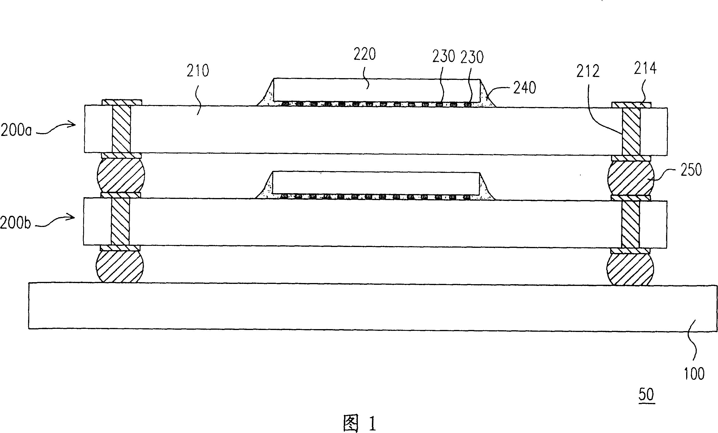
Chip packaging body without kernel dielectric layer and stack chip packaging structure
A chip packaging and packaging colloid technology, which is applied to electric solid devices, circuits, electrical components, etc., can solve the problem that the overall thickness of the stacked chip packaging structure 50 is reduced, the packaging accumulation of the stacked chip packaging structure 50 cannot be effectively improved, and Chip package thickness reduction barriers and other issues
- Summary
- Abstract
- Description
- Claims
- Application Information
AI Technical Summary
Problems solved by technology
Method used
Image

Examples
no. 1 example
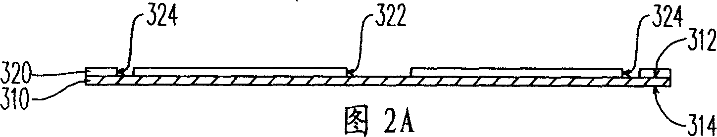
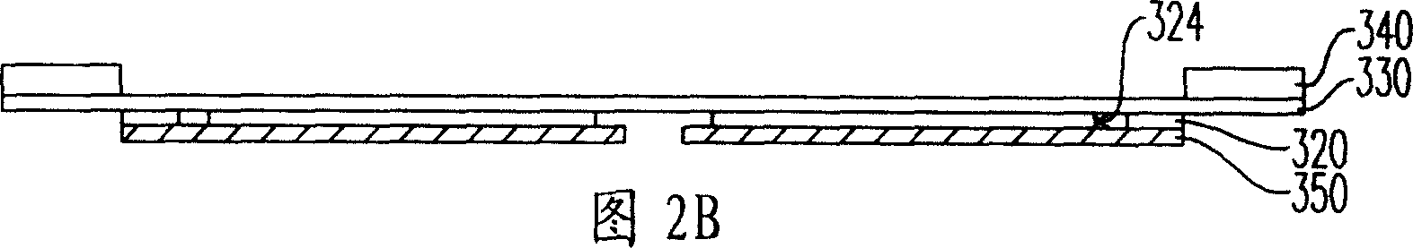
[0043] 2A-2F are schematic flow charts of the chip package process according to the first embodiment of the present invention. Referring to FIG. 2A , firstly, a conductive layer 310 is provided, wherein the conductive layer 310 has a first surface 314 and a second surface 312 opposite to each other, and the material of the conductive layer 310 is copper. Next, a solder mask layer 320 is formed on the second surface 312, and the solder mask layer 320 is patterned, for example, by means of lithography and etching to form a second opening 322 and a plurality of first openings 324, wherein the second opening 322 The first opening 324 exposes a part of the conductive layer 310 . In a preferred embodiment, in this embodiment, the conductive layer 310 can be treated with brown oxidation or black oxidation to improve the surface roughness of the conductive layer 310 and make the conductive layer 310 The bonding with the solder mask layer 320 is better.
[0044] Please refer to FIG. ...
no. 2 example
[0052] In the chip packaging process, the chip 360 can be electrically connected to the patterned circuit layer 350 through the wire bonding technology as disclosed in the first embodiment, and can also be packaged with flip chip technology or thin film chip. (chip on flex, COF) technology or other technologies to complete the electrical connection between the chip 360 and the patterned circuit layer 350 . The following will illustrate with an example the chip package process using the flip-chip technology.
[0053] 3A to 3E are schematic flowcharts of the chip package process according to the second embodiment of the present invention. Referring to FIG. 3A , firstly, a conductive layer 310 is provided, wherein the conductive layer 310 has a second surface 312 and a first surface 314 opposite to each other. Next, a solder mask layer 320 is formed on the second surface 312, and the solder mask layer 320 is patterned, for example, by using lithography and etching processes to f...
no. 3 example
[0059] In addition to the chip packages 300 and 300', the chip package process disclosed in the present invention can produce another chip package suitable for making a stacked chip package structure, and the manufacturing method will be described in detail below.
[0060] 4A-4E are schematic flowcharts of the chip package process according to the third embodiment of the present invention. Please refer to FIG. 4A , firstly, a conductive layer 310 is provided, wherein the conductive layer 310 has a second surface 312 and a first surface 314 opposite to each other. Next, a solder mask layer 320 is formed on the second surface 312, and the solder mask layer 320 is patterned, for example, by using lithography and etching processes to form a second opening 322 and a plurality of first openings 324, wherein the second opening 322 and the first opening 324 are formed. An opening 324 exposes a portion of the conductive layer 310 . In a preferred embodiment, in this embodiment, the co...
PUM
 Abstract
Description
Claims
Application Information