

Electron emitting device and manufacturing method thereof and image pick up device or display device using electron emitting device
An electron emission device and electron emission technology, applied in the manufacture of electrode systems, manufacture of discharge tubes/lamps, image/graphic display tubes, etc.
- Summary
- Abstract
- Description
- Claims
- Application Information
AI Technical Summary
Problems solved by technology
Method used
Image

Examples
other Embodiment approach
[0079] (Electron emission devices of other embodiments)
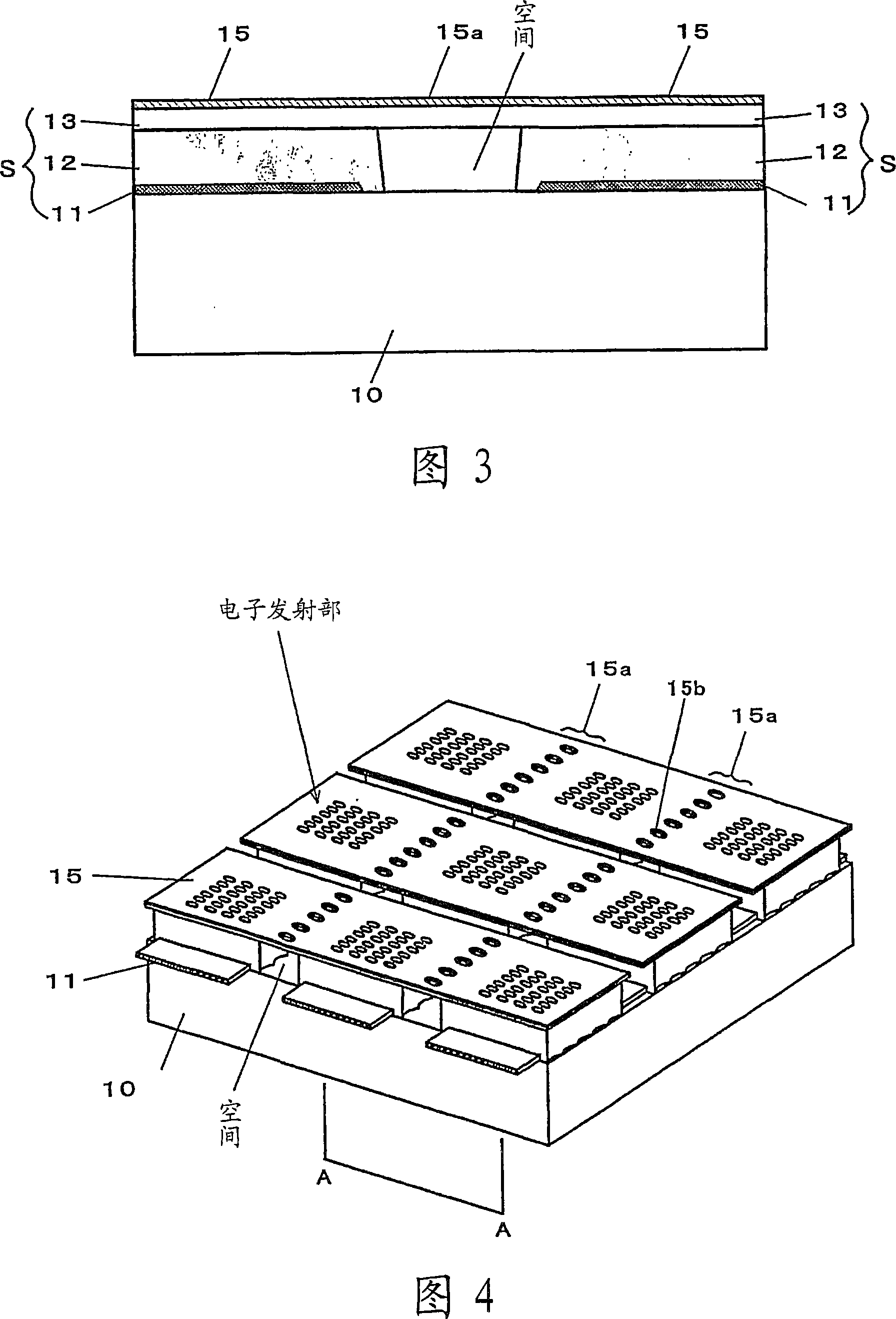
[0080] In the embodiment shown in FIG. 4 , in the pattern of the upper electrode 15, the elements are separated by a row of a plurality of through holes 15b, but in order to delineate the bridge portion 15a and separate the elements, for example, as shown in FIG. It is a bridge portion 15a having a notch portion 15c that narrows the width of the upper electrode 15 ( FIG. 20A ). Furthermore, as shown in FIG. 20B , a bridge portion 15a having a through hole 15b and a notch portion 15c may be used. In addition, as shown in FIG. 20C , in order to make all the upper electrodes 15 have the same potential, via holes 15 b may be provided in the xy direction, or bridge portions 15 a may be provided in the xy direction. The structure shown in FIG. 20C is effective in an active matrix driving method for electron emission devices in which electric power is supplied to each lower electrode. In addition, in addition to the circular...
Embodiment 1
[0094] SiO 2 On the Si wafer substrate covered with an insulating film, a thin film made of Al-Si serving as the bottom layer of the lower electrode is formed in stripes.
[0095] Then, no special patterning is required on the entire lower electrode where the electron emission element is to be arranged. Instead, a TiN lower electrode is formed with a film thickness of 220 nm by reactive sputtering by introducing nitrogen gas, and on the upper surface of the lower electrode , and an electron supply layer made of Si was formed with a film thickness of 5000 nm. This TiN layer functions as a lower electrode, and at the same time, can prevent Si diffusion from the Al—Si layer under the TiN layer to the electron supply layer formed on the TiN layer.
[0096] Then, a plurality of micromasks (see FIGS. 8 to 11 ) were fabricated so as to form island regions of electron emission portions on the electron supply layer on the obtained substrate.
[0097] Then, on the micromask and the el...
Embodiment 2
[0108] MOSFETs (MOS Field Effect Transistors) are arranged at positions corresponding to electron emission elements on the Si wafer substrate by known photolithography and etching techniques. Then, an interlayer insulating film was formed so as to cover a portion corresponding to a plurality of electron emission elements, and a lower electrode was formed on the interlayer insulating film. At this time, an opening penetrating to a position corresponding to each electron emission element is provided in the interlayer insulating film, and the drain electrode formed in the MOSFET is connected to the lower electrode through the opening.
[0109] After the lower electrode is individually separated for each electron emission element, an electron supply layer made of Si is formed to cover a portion corresponding to a plurality of electron emission elements without special patterning.
[0110] Then, on the obtained electron supply layer, an island region of the electron emission portio...
PUM
 Abstract
Description
Claims
Application Information