Production of flexible circuit board

A flexible circuit board and manufacturing method technology, applied in the direction of printed circuit, removal of conductive materials by chemical/electrolytic methods, printed circuit components, etc. The effect of solving the insufficient top width and avoiding the phenomenon of micro-short circuit

Inactive Publication Date: 2007-04-04
HIMAX TECH LTD
View PDF0 Cites 3 Cited by
  • Summary
  • Abstract
  • Description
  • Claims
  • Application Information

AI Technical Summary

Problems solved by technology

When wet etching is used to form the copper metal wires 210, because the nickel-chromium alloy is less likely to be etched than copper metal, so when etching the alloy layer 202, if the etching time is insufficient, the alloy layer between the copper metal wires 210 cannot be completely removed. , will cause a micro-short between the copper metal wires 210; if the etching time is increased in order to confirm that the alloy layer between the copper meta

Method used


Image

  • Production of flexible circuit board
  • Production of flexible circuit board
  • Production of flexible circuit board

Examples


Embodiment Construction

[0023] In order to make the flexible circuit board manufacturing method of the grain soft film bonding manufacturing process provided by the present invention more clear, how to form a copper metal wire structure with an appropriate top width on the flexible circuit board is described in detail in the embodiment of the present invention.

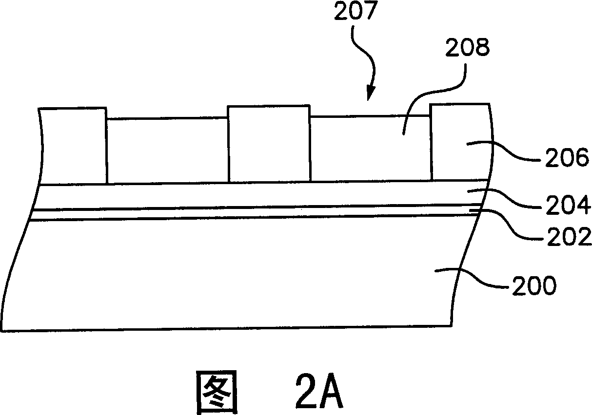
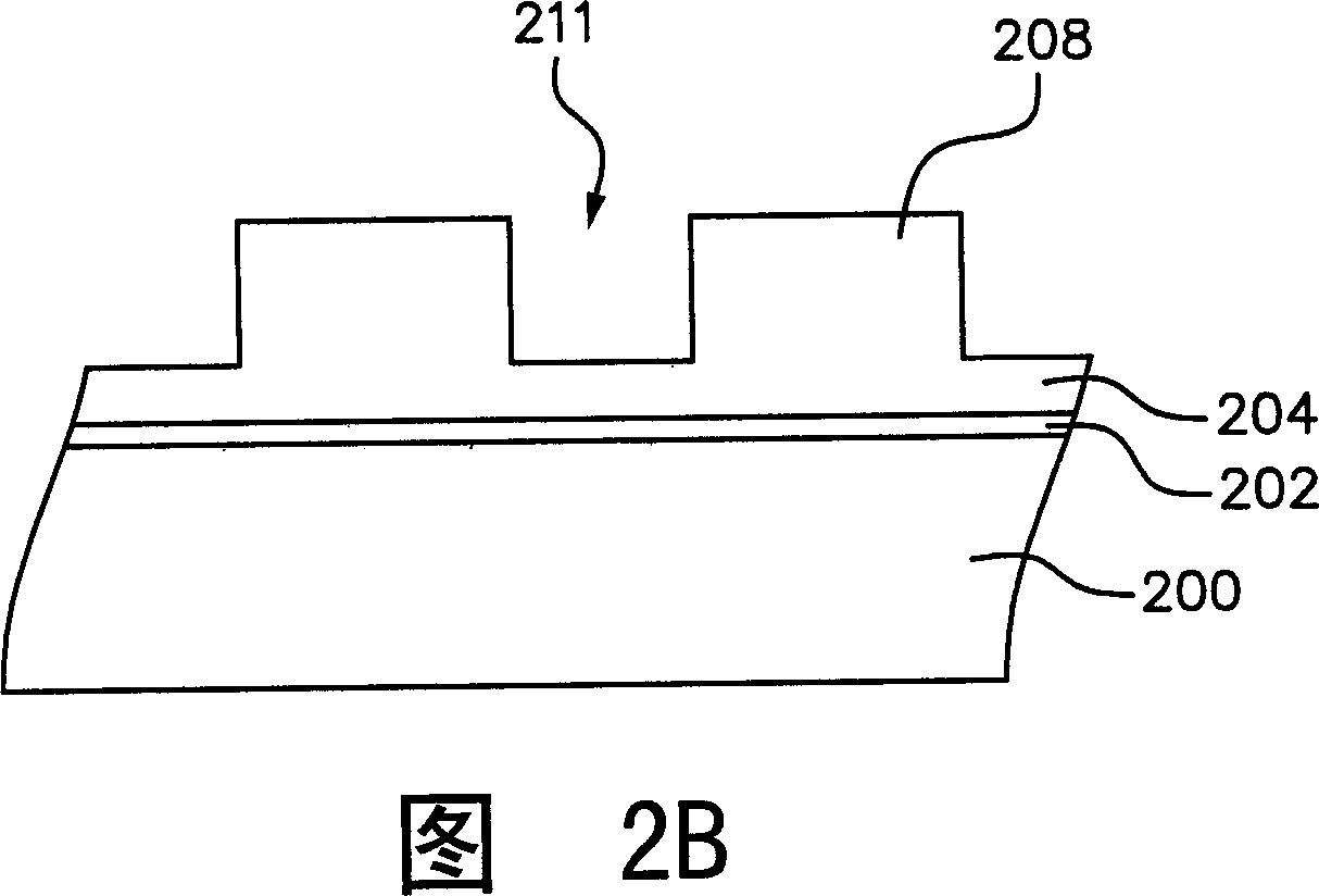
[0024] 3A to 3E are schematic cross-sectional views illustrating the manufacturing process of the flexible circuit board according to the embodiment of the present invention. Referring to FIG. 3A , an alloy layer 302 and a copper metal layer 304 are sequentially provided on a PI substrate 300 . Wherein, the material of the alloy layer 302 may be nickel-chromium alloy, and there is a copper seed layer (not shown in the figure) between the copper metal layer 304 and the alloy layer 302 . A patterned photoresist layer 306 is formed on the copper metal layer 304 , and the patterned photoresist layer 306 has openings 307 . Using the patterned ph...


PUM


Abstract

The method comprises: providing a flexible baseplate made by sequentially stacking a polyamide baseplate, an alloy layer and a first copper layer; making first photo etching, and patterning the first copper layer and the alloy layer in order to form multi first conducting wire structures on the polyamide baseboard; forming second copper layer on the polyamide baseplate and the first conducting wire structures; finally, making the second photo etching to remove the second copper layer on the polyamide baseplate.

Description

【Technical field】 [0001] The present invention relates to a method for manufacturing a flexible circuit board with a grain soft film bonding manufacturing process, and in particular to a method for manufacturing a copper structure on a flexible circuit board with a grain soft film bonding manufacturing process. 【Background technique】 [0002] The development of driver IC packaging technology has evolved from the Tape Automatic Bonding Process (TAB Process) to the Chip On Flex or Chip On Film Process (COF Process). The driving force of the display comes from the continuous improvement of display resolution and the increasingly thinner and smaller portable devices suitable for the display. [0003] The chip soft film bonding manufacturing process (COF Process) is a technology for flip chip bonding (Flip Chip Bonding) on ​​a flexible circuit board (Flexible or Film Printed Circuit board, FPC) substrate. That is, the driver chip (IC) and its electronic components can be placed ...

Claims


Application Information

Patent Timeline
IPC IPC(8): H05K3/06H05K1/09H05K1/00
Inventor 伍家辉郑百盛王宏倚
Owner HIMAX TECH LTD
Why Eureka
Try Eureka