Wafer processing device and wafer processing method

A wafer processing and wafer technology, which is applied in the field of wafer processing apparatus and wafer processing, can solve the problems of reduced processing efficiency, inability to cut accurately, and entrapped air bubbles, etc., and achieve the effects of improving processing efficiency and simplifying temperature control.

Inactive Publication Date: 2007-04-04
LINTEC CORP
View PDF1 Cites 8 Cited by
  • Summary
  • Abstract
  • Description
  • Claims
  • Application Information

AI Technical Summary

Problems solved by technology

Therefore, in addition to being difficult to smoothly perform the cutting operation by the cutter, there is also a problem that the adhesive transfers to the blade edge region of the cutter during cutting, and is temporarily bonded to the wafer after cutting along the outer peripheral edge of the wafer. Wafer bonding sheet cannot be cut with good precision
[0009] In addition, there is also such a problem that since the first table for temporary bonding of the adhesive sheet is kept at the preliminary heating temperature, when an adhesive sheet having a larger planar area than the wafer is attached, the wafer may be damaged. The part of the adhesive sheet protruding from the outer peripheral edge of the wafer is firmly bonded to the table, and it is difficult to remove the unnecessary adhesive sheet part on the outer peripheral side after cutting the adhesive sheet along the outer edge of the wafer
On the other hand, if the above-mentioned useless adhesive sheet part is not bonded to the first stage at all, then the useless adhesive sheet part becomes a free state, so when the adhesive sheet is stuck o

Method used


Image

  • Wafer processing device and wafer processing method
  • Wafer processing device and wafer processing method
  • Wafer processing device and wafer processing method

Examples


Embodiment Construction

[0074] Embodiments of the present invention will be described below with reference to the drawings.

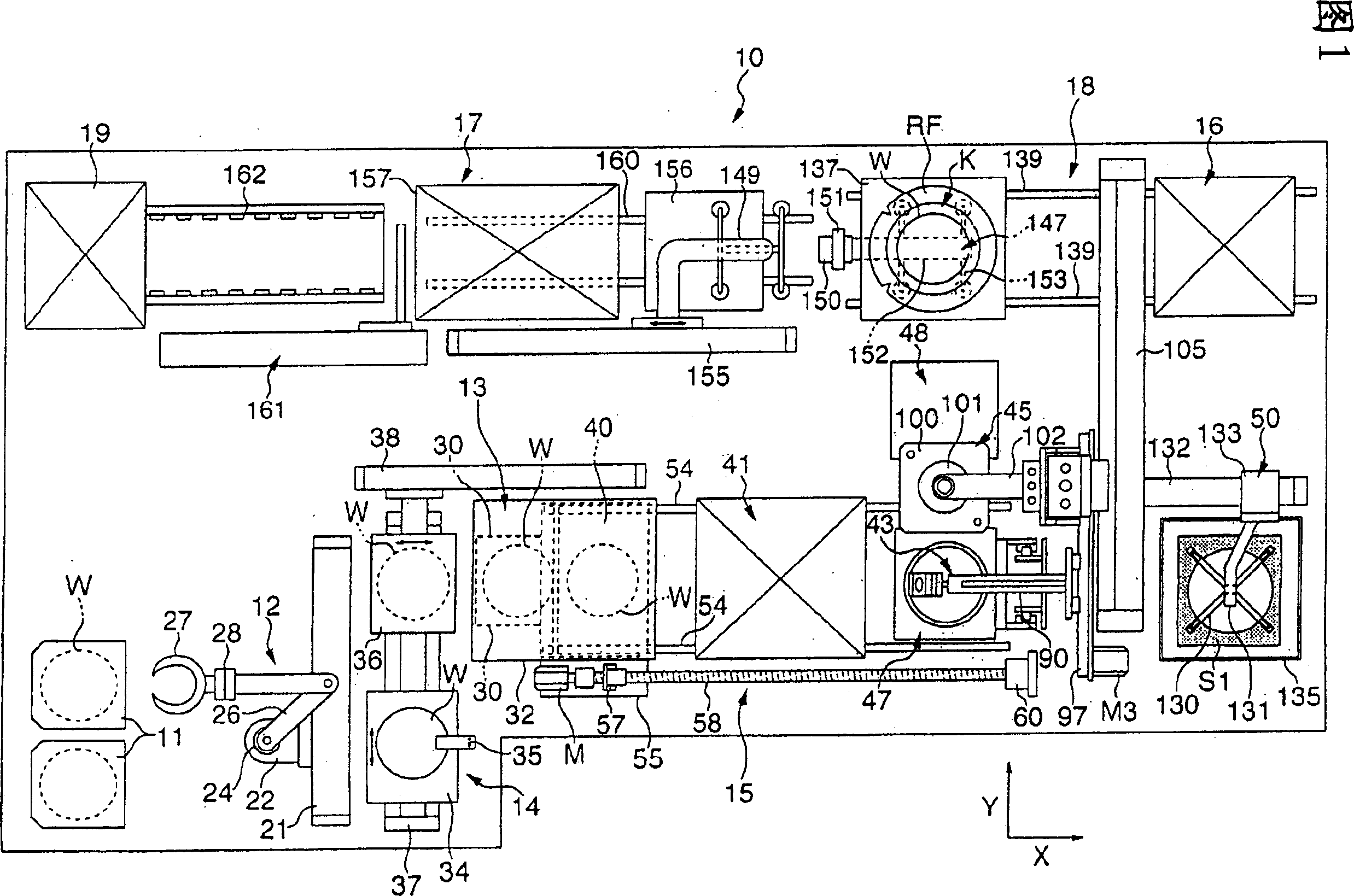
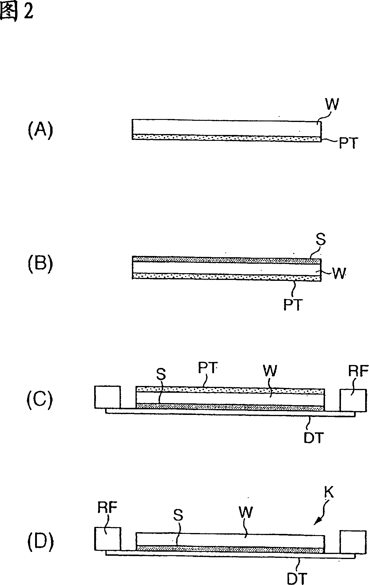
[0075] FIG. 1 is a plan view of a wafer processing apparatus according to this embodiment, and FIG. 2 is a schematic cross-sectional view illustrating wafer processing steps in chronological order. In these figures, the wafer processing apparatus 10 is constituted as an apparatus that performs a series of processes. The series of processes is aimed at a wafer W on which a UV-curable protective tape PT is attached to the surface constituting the circuit surface (see FIG. 2 ). ), after adhering a heat-sensitive adhesive sheet S for die bonding (hereinafter referred to as "adhesive sheet S" to the back surface of the wafer W, mount it on the ring frame RF via a dicing tape (Daishing Tape) DT Wafer W.

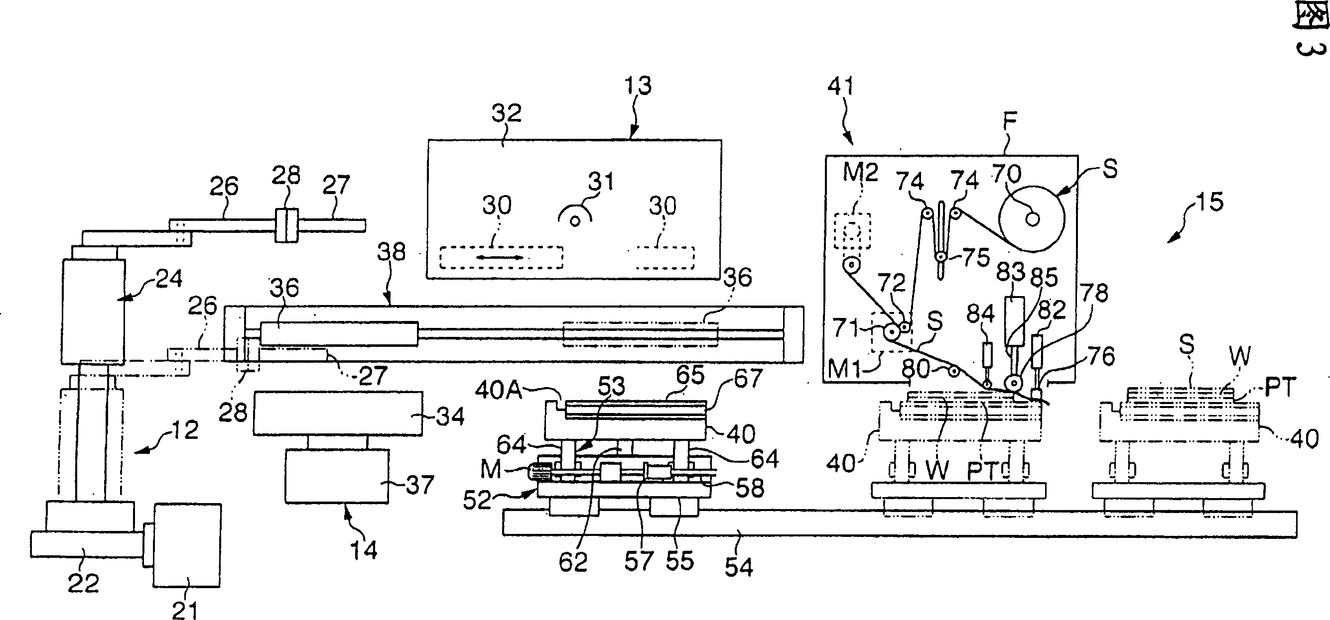
[0076] As shown in FIG. 1, the wafer processing apparatus 10 includes a cassette 11 for accommodating wafers W, a robot 12 for sucking and holding wafers W taken out of the casset...


PUM


Abstract

A sticking device (15) is constructed from a sticking table (40) supporting a semiconductor wafer (W), a sticking unit (41) for sticking a heat-sensitive adhesive sheet (S), and a cutter (96) for cutting the adhesive sheet crosswise and peripherally for each semiconductor wafer. The table comprises the first sticking table (40) controlled to a first temperature for temporarily sticking the adhesive sheet (S) to the wafer (W), an outer periphery cutting table (47) controlled to a second temperature which lowers the stickiness of the adhesive sheet for cutting the latter, and a connecting table (48) controlled to a third temperature for completely sticking the adhesive sheet (S) to the wafer (W).

Description

technical field [0001] The present invention relates to a wafer processing apparatus and a wafer processing method, in particular to a wafer processing apparatus capable of reliably bonding a heat-sensitive adhesive sheet to an adherend while cutting the heat-sensitive adhesive sheet according to the size of the adherend. Wafer handling methods. Background technique [0002] After the semiconductor wafer on which the circuit surface is formed (hereinafter referred to as "wafer") is separated into chips, each chip is picked up and bonded (die bonding) to a lead frame. This die bonding can be performed by attaching a thermally-adhesive adhesive sheet used for die bonding in advance in a wafer processing step. [0003] As an sticking device of such an adhesive sheet, it is disclosed by patent document 1, for example. The sticking device disclosed in this document has a first table, a sheet supply device, a pressure roller, a cutter, a second table, and a heating device; Prel...

Claims


Application Information

Patent Timeline
IPC IPC(8): H01L21/68H01L21/301B29C65/50B29L7/00B29L9/00B29L31/34H01L21/683
Inventor 辻本正树吉冈孝久小林贤治
Owner LINTEC CORP
Why Eureka
Try Eureka