

Display device
A technology for display devices and converters, which is applied to static indicators, image communications, electrical components, etc., can solve the problems of rising manufacturing costs of drive control circuits and rising costs of display devices, and achieve suppression of complexity and cost of manufacturing processes The effect of preventing the rise of the threshold voltage and the fluctuation of the threshold voltage
- Summary
- Abstract
- Description
- Claims
- Application Information
AI Technical Summary
Problems solved by technology
Method used
Image

Examples
Embodiment approach 1
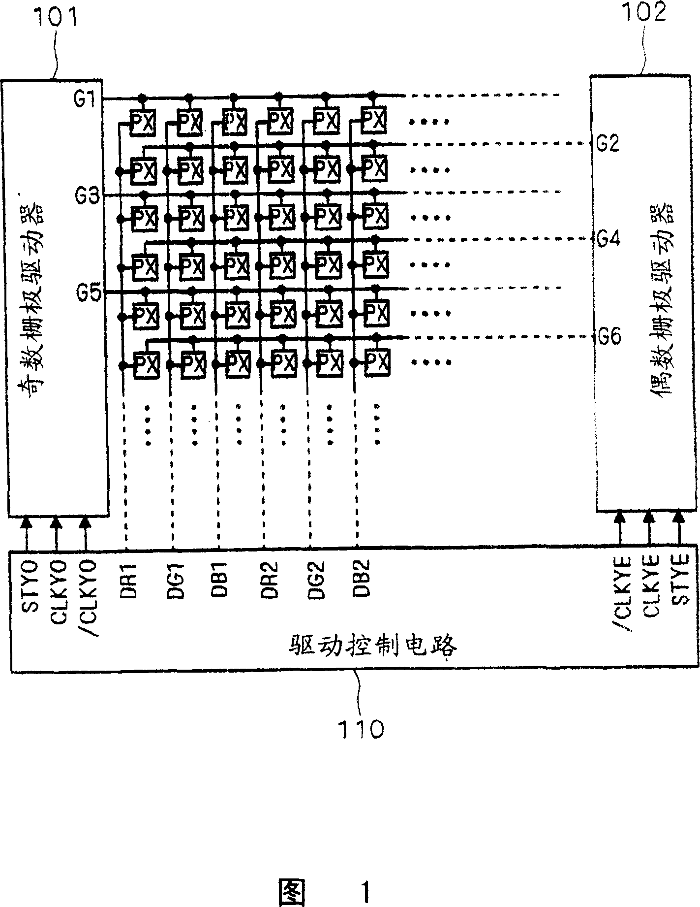
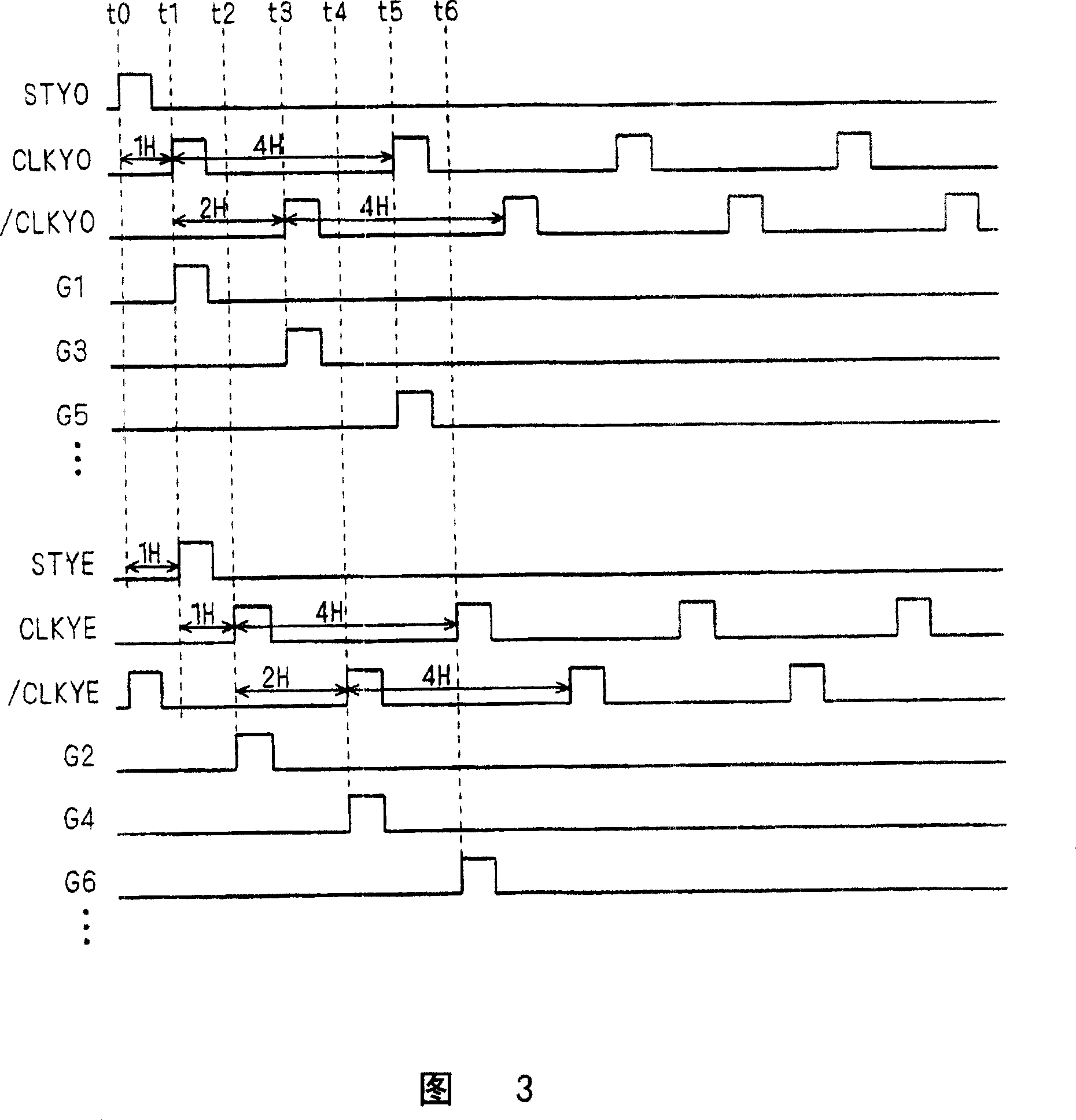
[0038] Next, specific embodiments of the present invention will be described. In order to facilitate the understanding of the present invention, first, conventional general-purpose drive control circuits and gate drivers will be described. FIG. 1 is a block diagram showing a configuration example of a conventional display device.
[0039] In the display device of FIG. 1 , pixels PX composed of a-Si TFTs formed on an insulating substrate such as glass are arranged in a matrix. Examples of the pixel PX include a pixel using a liquid crystal element, a pixel using an electroluminescent element such as organic EL (electroluminescence), and the like.
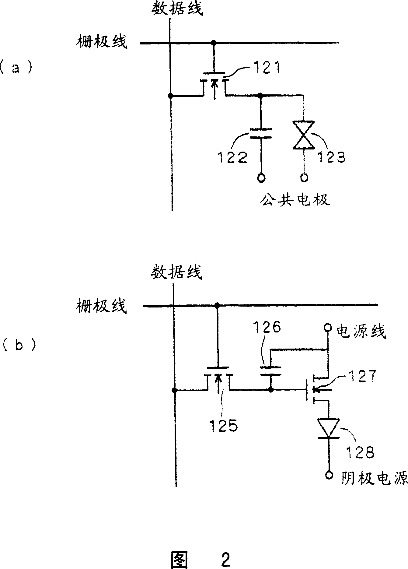
[0040] FIG. 2( a ) is a structural example of a liquid crystal pixel using a-Si TFT. The gate of the active element 121 (a-Si TFT) is connected to the gate line, and the drain of the active element 121 is connected to the data line. In addition, the storage capacitor 122 and the liquid crystal element 123 are connected to the sourc...
Embodiment approach 2
[0126] In Embodiment 2, an example of the circuit configuration of the frequency dividing circuit 20 different from that in FIG. 7 is shown.
[0127] FIG. 12 is a diagram showing a circuit configuration of a frequency dividing circuit 20 a according to the second embodiment.
[0128] The frequency dividing circuit 20a is different from the frequency dividing circuit 20 of FIG. 7 in that a transistor 26 is provided between the input terminal of the start signal STYE and the node N5. That is, the frequency dividing circuit 20a has a latch converter 23a composed of transistors Q10 to Q13, Q26 between the nodes N1 and N5 instead of the latch converter 23 of FIG. 7 .
[0129] FIG. 13 is a timing chart showing the operation of the frequency division circuit 20a, showing transition from a state where the frequency division signal VFR is at H level and the frequency division signal / VFR is at L level to the state where the frequency division signal VFR is at L level and the frequency ...
Embodiment approach 3
[0132] Embodiment 3 also shows an example of the circuit configuration of the frequency dividing circuit 20 different from that in FIG. 7 . FIG. 14 is a diagram showing a circuit configuration of a frequency dividing circuit 20b according to the third embodiment. In the frequency dividing circuit 20b of FIG. 14, a buffer 29 is provided instead of the transistor Q1 of FIG. 7, and a buffer 22a is provided instead of the buffer 22 and the transistor Q9 of FIG. Other configurations are the same as in FIG. 7 .
[0133] The buffer 29 is composed of a buffer circuit composed of transistors Q18a and Q19a, a transistor Q1a connected between the buffer circuit and the input terminal of the start signal STYO, and a transistor Q1b connected between the buffer circuit and the low potential side power supply. . The gate of the transistor Q18a is connected to the gate of the transistor Q18 (node N7), and the gate of the transistor Q19a is connected to the gate of the transistor Q19 (node...
PUM
 Abstract
Description
Claims
Application Information