

Method for preparing LED electrode
A technology for manufacturing light-emitting diodes and electrodes, which is applied in the direction of circuits, electrical components, semiconductor devices, etc., can solve the problem of wire plate falling off, etc., and achieve the effect of firm adhesion
- Summary
- Abstract
- Description
- Claims
- Application Information
AI Technical Summary
Problems solved by technology
Method used
Image

Examples
Embodiment 1
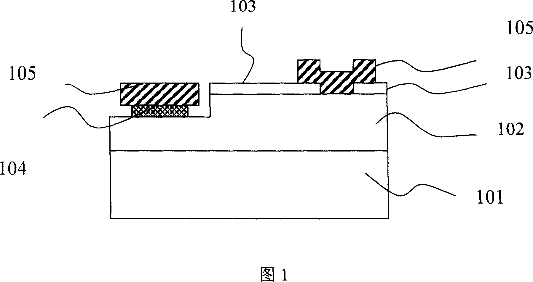
[0025] An electrode structure and manufacturing method of a gallium nitride light-emitting diode chip includes the following processes, and the structure refers to FIG. 2:
[0026] 1. Grow N-type gallium nitride (202) and P-type gallium nitride (203) on a sapphire substrate (201), and then vapor-deposit Ni / The Au metal layer (204), with a thickness of 50-500 Ȧ, is then annealed in an air environment at a temperature of 250-700° C. for 10-40 minutes to form a transparent P-type ohmic contact layer; and then evaporated by an electron beam Method A Ti / Ni / Al metal layer (205) is vapor-deposited on the N+ layer of the gallium nitride epitaxial wafer with a thickness of 100-5000 Ȧ to form an N-type ohmic contact layer.
[0027] 2. Use photolithography and wet etching to remove part of the ohmic contact electrode layer at the position where the P bonding pad is prepared, exposing the P-type gallium nitride epitaxial layer, whose size is smaller than the size of the P bonding pad.
...
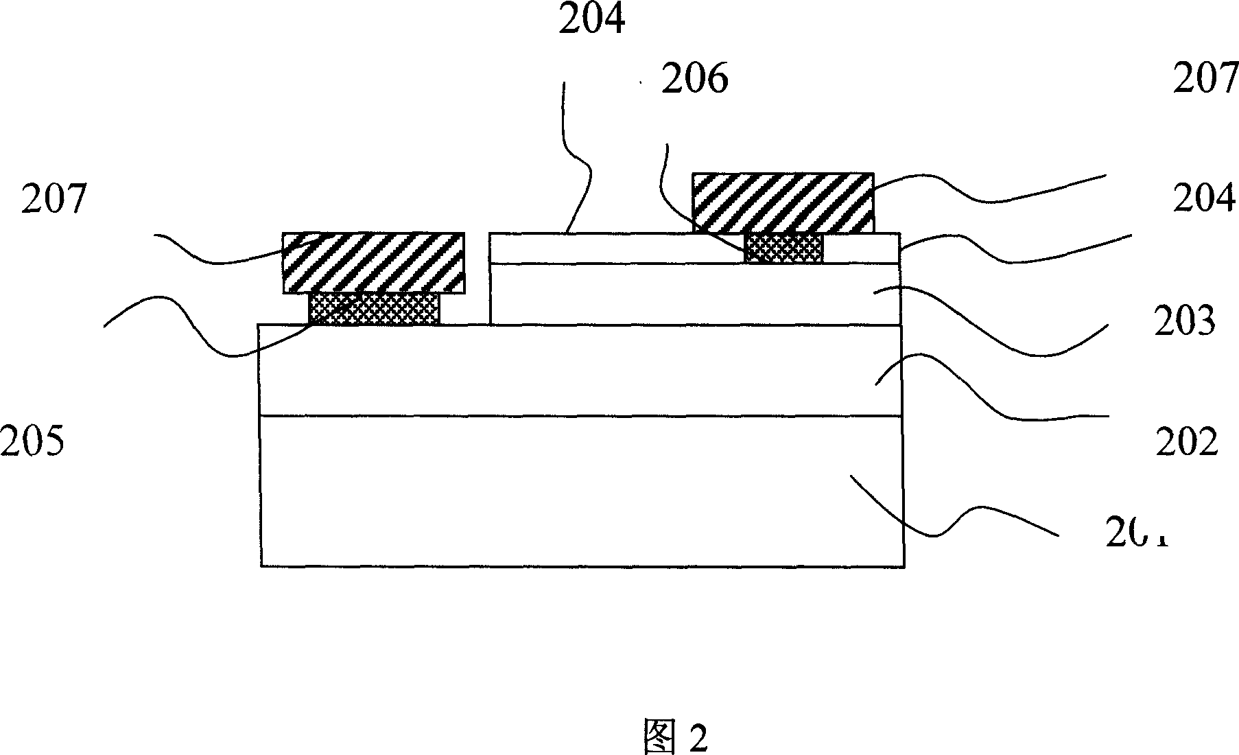
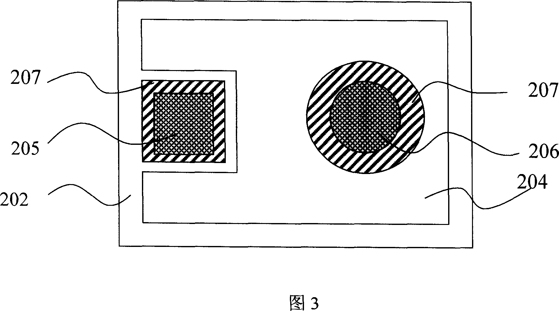
Embodiment 2
[0035] An electrode structure and manufacturing method of a gallium nitride light-emitting diode chip includes the following processes, and the structure refers to FIG. 4:
[0036] 1. Grow N-type gallium nitride (202) and P-type gallium nitride (203) on a sapphire substrate (201), and then vapor-deposit Ni / The Au metal layer (204), with a thickness of 50-500 Ȧ, is then annealed in an air environment at a temperature of 250-700° C. for 10-40 minutes to form a transparent P-type ohmic contact layer; and then evaporated by an electron beam Method A Ti / Ni / Al metal layer (205) is vapor-deposited on the N+ layer of the gallium nitride epitaxial wafer with a thickness of 100-5000 Ȧ to form an N-type ohmic contact layer.
[0037] 2. Use photolithography and wet etching to remove part of the ohmic contact electrode layer at the position where the P bonding pad is prepared, exposing the P-type gallium nitride epitaxial layer, whose size is smaller than the size of the P bonding pad.
[...
PUM
 Abstract
Description
Claims
Application Information