Method for preparing wave guide and grating structure of adjustable distributive feedback quantum cascade laser and above said grating
A technology of distributed feedback and quantum cascade, which is applied to the structure of optical waveguide semiconductors, the structure of optical resonators, lasers, etc., can solve the problem of increased laser threshold current density, strong coupling between laser modes and plasmons, and increased laser waveguide Loss and other issues
- Summary
- Abstract
- Description
- Claims
- Application Information
AI Technical Summary
Problems solved by technology
Method used
Image
Examples
Embodiment 1
[0041] Example 1 8.4 μm InGaAs / AlInAs / InP distributed feedback quantum cascade laser
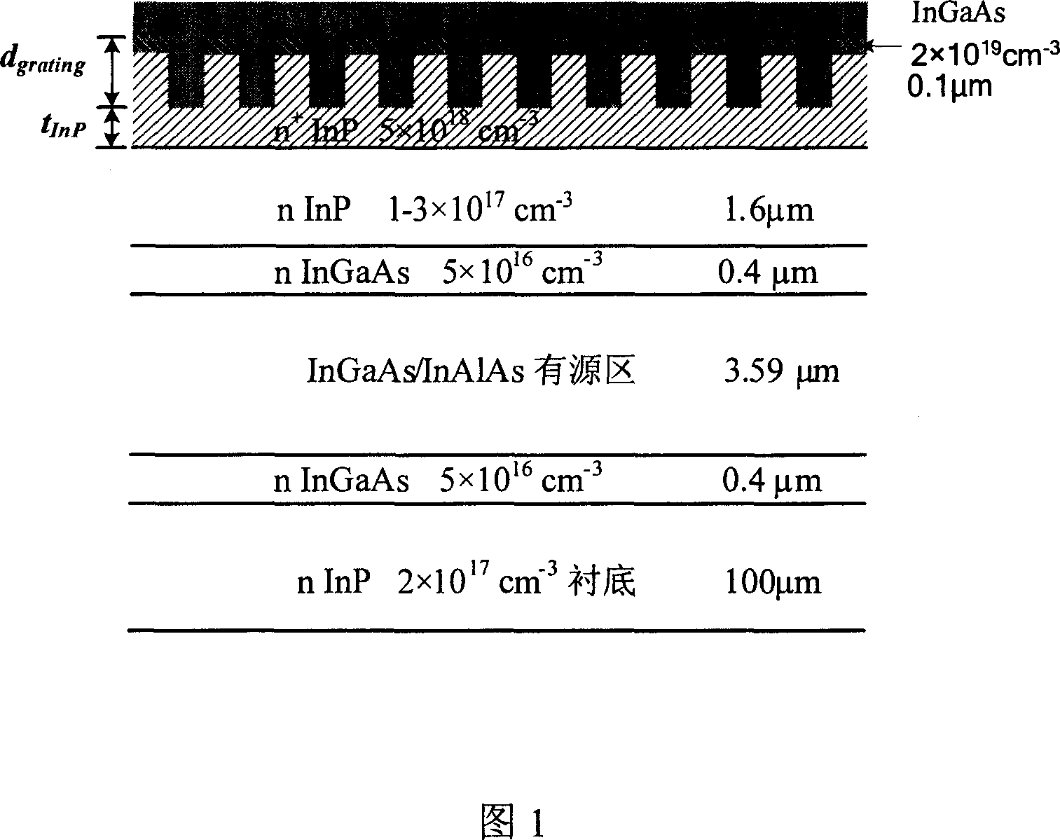
[0042] Fig. 1 is a schematic diagram of a waveguide and grating structure of an InGaAs / AlInAs / InP tunable distributed feedback quantum cascade laser with a wavelength of 8.4 μm. The active layer region includes 60 periods of "active layer + injection region" structure with a thickness of 3.59 μm. The thickness of the upper and lower active regions is 0.4 μm, and the n-type doping concentration is 5×10 16 cm -3 InGaAs waveguide layer. Above the upper waveguide layer is an n-type moderately doped confinement layer InP (1-3×10 17 cm -3 , thickness 1.6μm), n-type heavily doped InP confinement layer (5×10 18 cm -3 , thickness 1.0μm), and n-type heavily doped InGaAs capping layer (2×10 19 cm -3 , thickness 0.1 μm). The substrate is moderately doped n-type InP (2×10 17 cm -3 ).
[0043] Using the method described in the summary of the invention in the specification of the invention, the...
Embodiment 2
[0048] Example 2 7.7 μm InGaAs / AlInAs / InP distributed feedback quantum cascade laser
[0049] Figure 6 shows the waveguide structure of an InGaAs / InP tunable distributed feedback quantum cascade laser with a laser wavelength of 7.7 μm. The active layer region includes 60 periods of "active layer + injection region" structure with a thickness of 2.66 μm. The thickness of the upper and lower active regions is 0.7μm, and the n-type doping concentration is 5×10 16 cm -3 InGaAs waveguide layer. Above the upper waveguide layer is an n-type moderately doped confinement layer InP (1-3×10 17 cm -3 , thickness 1.6μm), n-type heavily doped InP confinement layer (5×10 18 cm -3 , thickness 0.7μm), and n-type heavily doped InGaAs cap layer (2×10 19 cm -3 , thickness 0.1 μm). The substrate is moderately doped n-type InP (2×10 17 cm -3 ).
[0050] According to the same design principle and combined with numerical calculations, we designed the thickness of the heavily doped InGaAs ...
PUM
 Abstract
Description
Claims
Application Information


