Plasma treatment device

A plasma and processing device technology, which is applied in the field of substrate devices, can solve problems such as processing chamber pollution, and achieve the effect of reducing density

Active Publication Date: 2007-04-18
ADVANCED MICRO FAB EQUIP INC CHINA
View PDF4 Cites 20 Cited by
  • Summary
  • Abstract
  • Description
  • Claims
  • Application Information

AI Technical Summary

Problems solved by technology

[0006] The purpose of the present invention is to provide a plasma processing device, which overcomes the deficiencies of the prior art and solves the problem of contamination of the processing chamber of the plasma processing device caused by plasma diffusion

Method used


Image

  • Plasma treatment device
  • Plasma treatment device
  • Plasma treatment device

Examples


Embodiment Construction

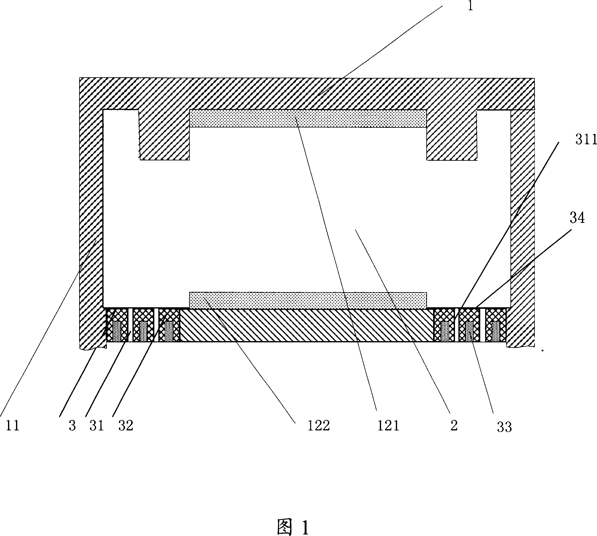
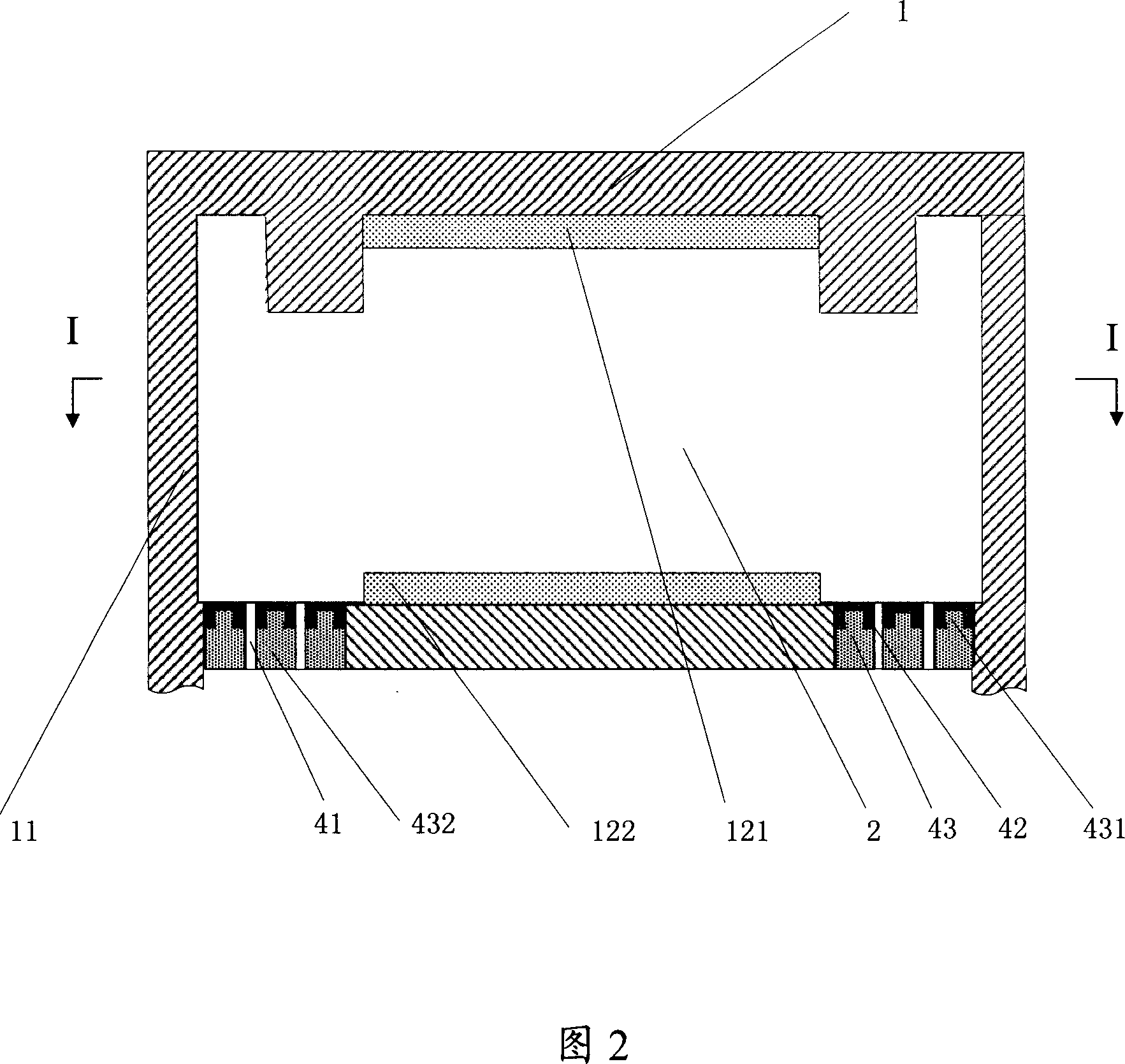
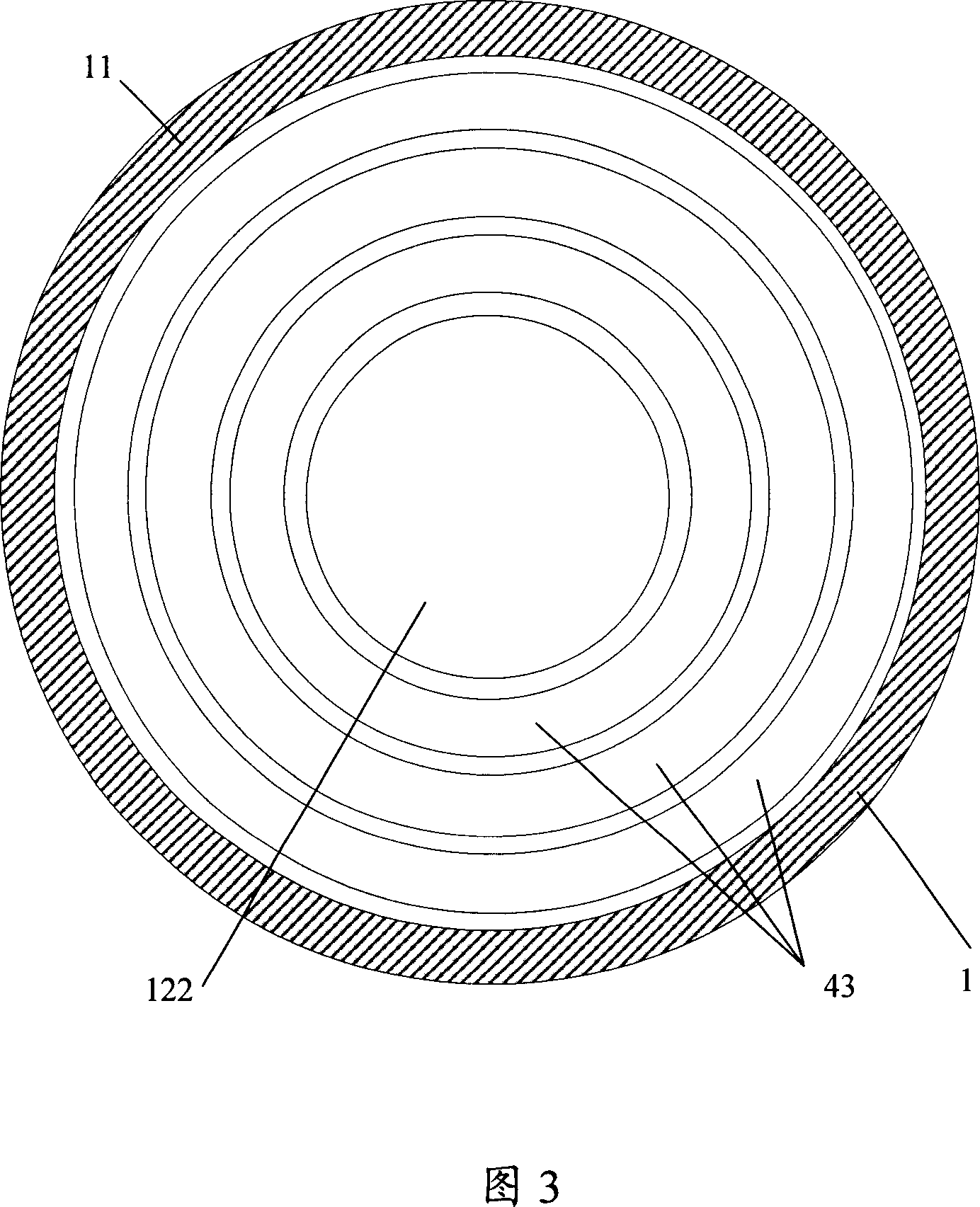
[0050] Please refer to FIG. 1 . FIG. 1 is a schematic structural diagram of an embodiment of the plasma processing apparatus of the present invention. In this embodiment, the plasma processing apparatus 1 has a processing chamber 11, the processing chamber 11 is substantially cylindrical, and the side walls of the processing chamber are substantially vertical, and there are upper electrodes arranged parallel to each other in the processing chamber 11. 121 and the lower electrode 122. Generally, the area 2 between the upper electrode 121 and the lower electrode 122 is the processing area, which will generate high frequency energy to ignite and maintain the plasma. A workpiece to be processed is placed above the lower electrode 122, and the workpiece may be a semiconductor substrate to be etched or processed or a glass plate to be processed into a flat panel display. The reaction gas is input into the processing chamber 11 from a gas injection port (not shown), and one or more ...


PUM


Abstract

The invention offers a plasma processing unit equipped with plasma restraint device. The plasma restraint device contains many insulating elements which are set with intervals and form slender channels. Small parts of insulating elements have at least one conductive element inside. The conductive elements electric connect with each other and put to earth to form electric-field mask. The invention efficiently solves problems that cavity pollution of plasma processing unit led by plasma diffusing and secondary plasma discharge outside processing area.

Description

Technical field [0001] The present invention relates to an apparatus for processing semiconductor substrates for integrated circuits or glass flat substrates for flat panel displays, and more particularly to a plasma processing apparatus equipped with a plasma confinement device. Background technique [0002] The plasma processing device uses the working principle of the vacuum reaction chamber to process the semiconductor substrate and the substrate of the plasma flat panel. The working principle of the vacuum reaction chamber is to pass a reaction gas containing an appropriate etchant or deposition source gas into the vacuum reaction chamber, and then input radio frequency energy to the vacuum reaction chamber to activate the reaction gas to ignite and maintain the plasma body, in order to respectively etch the material layer on the surface of the substrate or deposit the material layer on the surface of the substrate, and then process the semiconductor substrate and the p...

Claims


Application Information

Patent Timeline
Patent Type & Authority Applications(China)
IPC IPC(8): C23C16/513
Inventor 倪图强
Owner ADVANCED MICRO FAB EQUIP INC CHINA
Why Eureka
Try Eureka