Superhigh strength high conduction block pure copper material and preparation method
A high-conductivity, ultra-high-strength technology, applied in the field of bulk high-density nano-twinned metal pure copper and its preparation, achieves the effects of simple preparation method, excellent conductivity and strong applicability
- Summary
- Abstract
- Description
- Claims
- Application Information
AI Technical Summary
Problems solved by technology
Method used
Image
Examples
Embodiment 1
[0027] Using high-speed deformation technology to prepare high-strength, high-conductivity bulk high-density nano-twinned pure copper materials;
[0028] Equipment: Pneumatic high-speed deformation equipment;
[0029] Deformation strain rate: 1×10 2 the s -1 ;
[0030] Deformation strain: deformation 2.3 (5 deformations, each deformation of the first four deformations is 0.5, and the fifth deformation is 0.3);
[0031] Deformation temperature: -196°C;
[0032] Pure copper material: purity 99.95%, annealed at 700°C for 3 hours, grain size 150-200 microns.
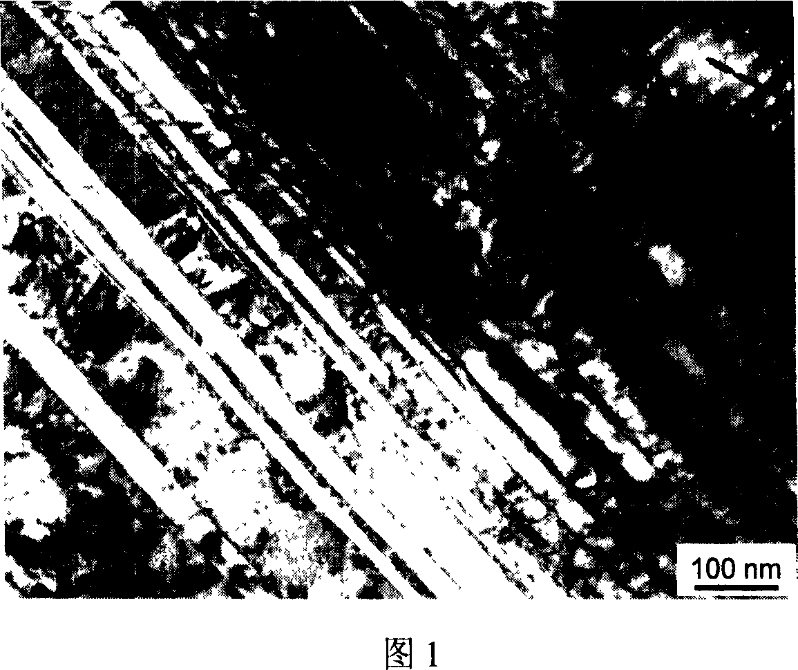
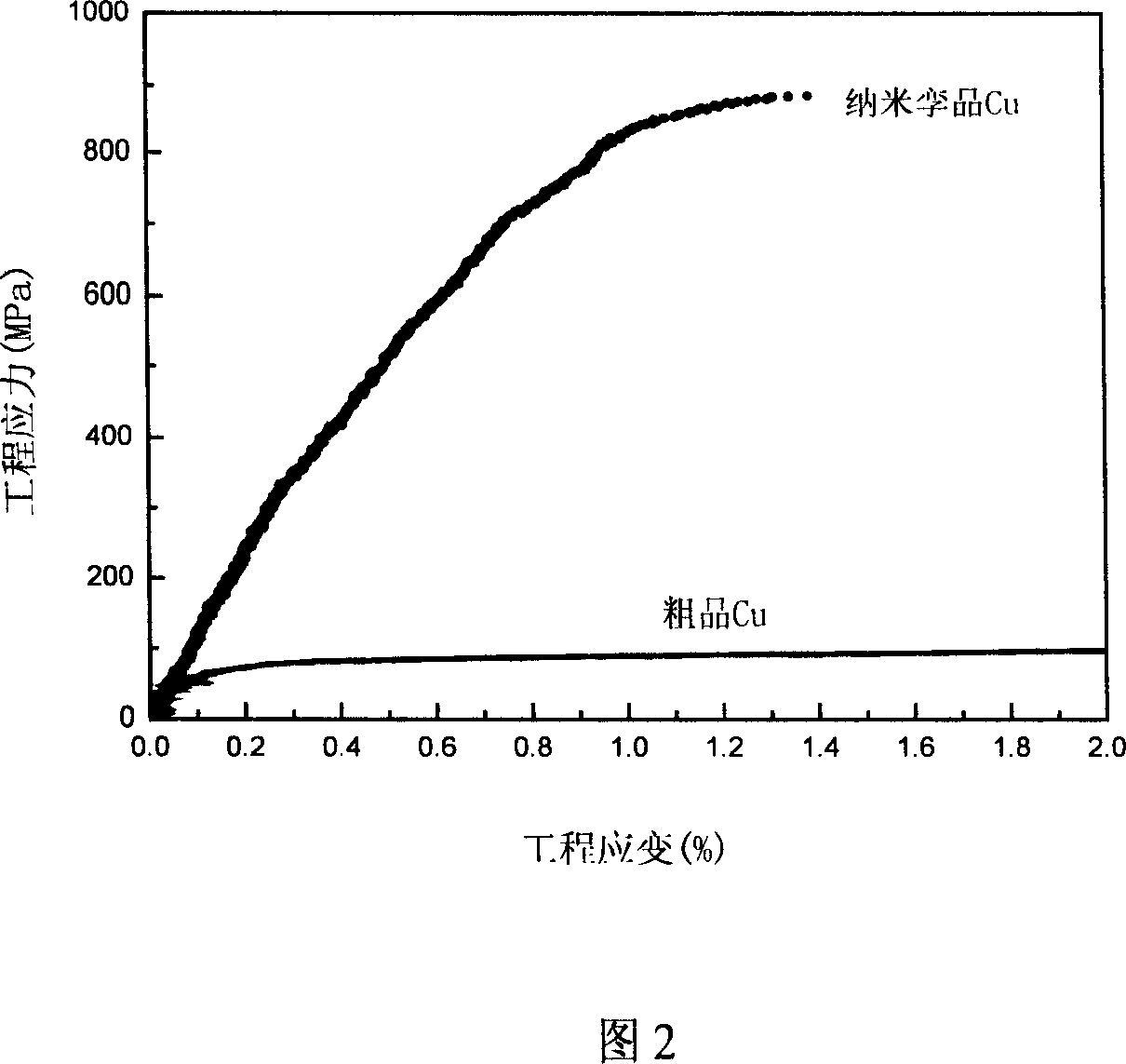
[0033] A bulk high-density nano-sized twinned pure copper material is prepared, as shown in Figure 1. The main feature of its microstructure is bundle-shaped high-density nano-mechanical twins, with an average twin layer thickness of 30-50 nanometers and a length of 200-800 nanometers. The twin density is about 3×10 7 m 2 / m 3 . There are high-density dislocations in both the matrix and the twins, and the dislocatio...
Embodiment 2
[0035] Using high-speed deformation technology to prepare high-strength, high-conductivity bulk high-density nano-twinned pure copper materials;
[0036] Equipment: Pneumatic high-speed deformation equipment;
[0037] Deformation strain rate: 1×10 3 the s -1 ;
[0038] Deformation strain: deformation 2 (4 deformations, each deformation 0.5);
[0039] Deformation temperature: -100°C;
[0040] Pure copper material: purity 99.95%, annealed at 700°C for 3 hours, grain size 150-200 microns.
[0041] A bulk high-density nano-sized twinned pure copper material is prepared, as shown in Figure 1. The main feature of its microstructure is bundled high-density nano-mechanical twins, with an average twin layer thickness of 30-50 nanometers and a length of 100-600 nanometers. The twin density is about 1.5×10 7 m 2 / m 3 . There are high-density dislocations in both the matrix and the twins, and the dislocation density is 1.3×10 15 . Using a strain rate of 6 x 10 -3 the s -1 A ten...
Embodiment 3
[0043] Using high-speed deformation technology to prepare high-strength, high-conductivity bulk high-density nano-twinned pure copper materials;
[0044] Equipment: Pneumatic high-speed deformation equipment;
[0045] Deformation strain rate: 1×10 4 the s -1 ;
[0046] Deformation strain: deformation 2.5 (5 deformations, each deformation 0.5);
[0047] Deformation temperature: -20°C;
[0048] Pure copper material: purity 99.95%, annealed at 700°C for 3 hours, grain size 150-200 microns.
[0049] A bulk high-density nano-sized twinned pure copper material is prepared, as shown in Figure 1. The main feature of its microstructure is bundle-shaped high-density nano-mechanical twins, with an average twin layer thickness of 30-50 nanometers and a length of 200-800 nanometers. The twin density is about 1.5×10 7 m 2 / m 3 . There are high-density dislocations in both the matrix and the twins, and the dislocation density is 1×10 15 . Using a strain rate of 6 x 10 -3 the s -...
PUM
| Property | Measurement | Unit |
|---|---|---|
| Deformation temperature | aaaaa | aaaaa |
| Thickness | aaaaa | aaaaa |
| Yield strength | aaaaa | aaaaa |
Abstract
Description
Claims
Application Information


