System and method for photolithography in semiconductor manufacturing

A technology of semiconductors and manufacturing methods, applied in semiconductor/solid-state device manufacturing, photography, microlithography exposure equipment, etc., can solve the problems of general products and methods without suitable structures and methods, inconvenience, etc.

A technology of semiconductors and manufacturing methods, applied in semiconductor/solid-state device manufacturing, photography, microlithography exposure equipment, etc., can solve the problems of general products and methods without suitable structures and methods, inconvenience, etc.

CN1955847AActive Publication Date: 2007-05-02TAIWAN SEMICON MFG CO LTD

Image

  • System and method for photolithography in semiconductor manufacturing
  • System and method for photolithography in semiconductor manufacturing
  • System and method for photolithography in semiconductor manufacturing

Examples


Embodiment Construction

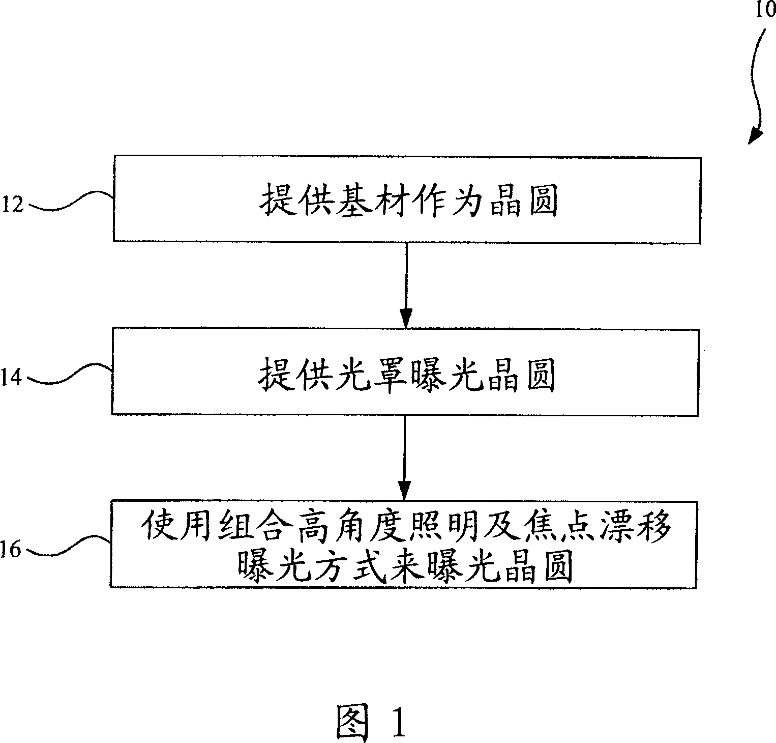
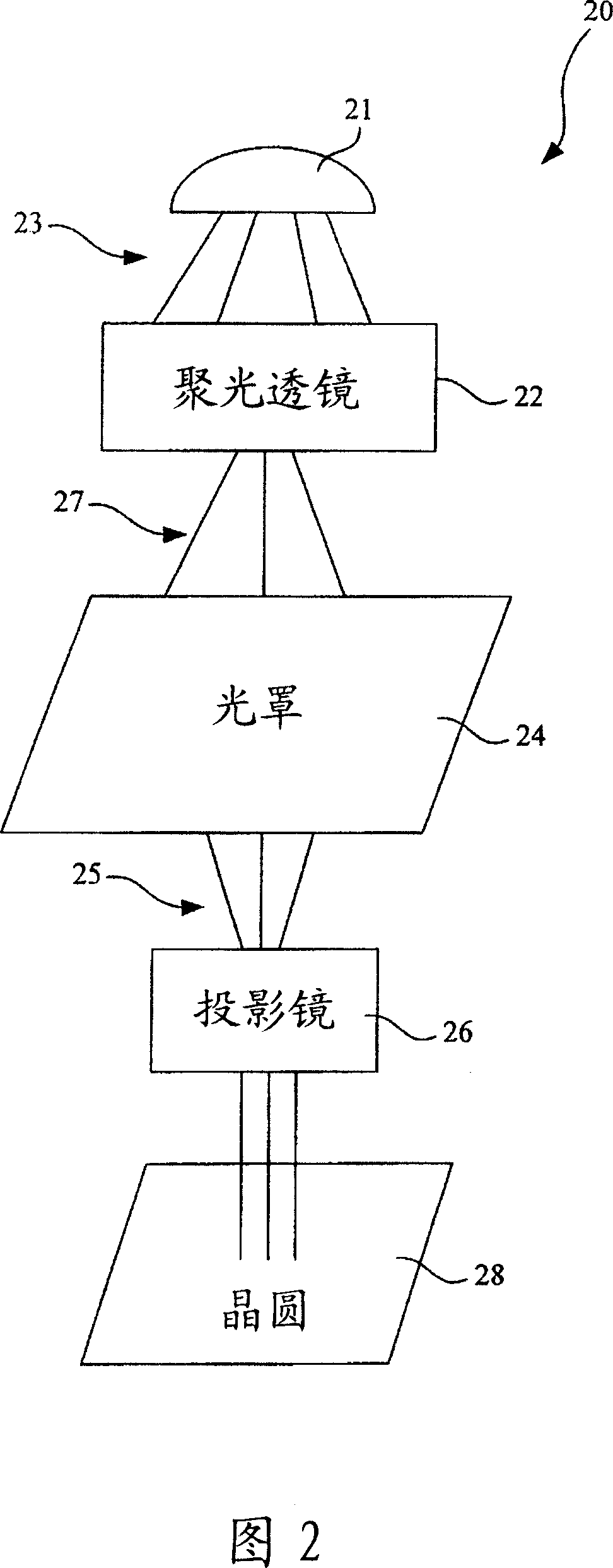
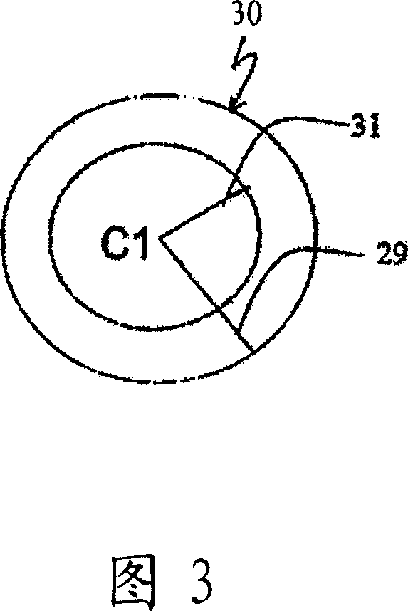
[0064] In order to further explain the technical means and effects of the present invention to achieve the intended purpose of the invention, the following in conjunction with the drawings and preferred embodiments, the specific implementation of the system and method for the semiconductor lithography process proposed according to the present invention, The structure, processing method, steps, features and functions thereof are described in detail below.

[0065] The invention to be disclosed next provides many different embodiments, or examples of the invention applied to different structures. Specific constituent samples, as well as designed parts, will be described below to make the present invention easy to understand. Of course, these examples are not intended to limit the present invention. In addition, some reference numerals or nouns are repeated in various embodiments of the present invention, which is for the purpose of simplifying and clearly understanding the pres...


PUM

PropertyMeasurementUnit
thicknessaaaaaaaaaa

Abstract

The present invention is relates to a method for photolithography in semiconductor manufacturing which includes providing a substrate for a wafer and providing a mask for exposing the wafer. The wafer is exposed by utilizing a combination of high angle illumination and focus drift exposure methods. The photolithography using the method of conforming high-angle illumination and a method of focus drift exposure, can reduce the proximity effect and increase the focus depth.

Description

technical field [0001] The present invention relates to a method for manufacturing a semiconductor element, in particular to a photolithography process applied in semiconductor manufacturing. Background technique [0002] When the semiconductor industry began to develop, photolithography was used to form components in integrated circuits. The density of components that can be placed on a single wafer also continues to increase due to the continuous advancement of photolithography technology, especially the decreasing wavelength of exposure radiation. As long as the critical dimensions of the circuit elements are larger than the wavelength of radiation used to expose the photoresist, the technology does not require any significant changes in the characteristics of the reticle. [0003] However, when the imaged radiation wavelength is larger than the critical dimension, the diffraction effect that has always existed becomes very obvious at this time, resulting in severe disto...

Claims


Application Information

Patent Timeline
02 May 2007
Publication
CN1955847A
IPC
G03F7/20; H01L21/027
CPC
G03F7/70641; G03F7/70108; G03F7/70333; G03F9/7026; G03F7/70283; G03F7/70091; G03F7/70308; G03F7/7055
Inventors
ι™ˆζ‘‚ι‘Ί; ζž—θΏ›η₯₯