A three-dimensional wafer stacking structure with post-and-beam construction and method to stack three-dimensional wafer

A technology of stacked structure and wafer, applied in the direction of electrical components, electric solid devices, circuits, etc., can solve the problems of thermal stress damage, chip circuit damage, inability to support the device layer, etc., to achieve the effect of stress-free damage

Active Publication Date: 2007-05-16
IND TECH RES INST
View PDF0 Cites 8 Cited by
  • Summary
  • Abstract
  • Description
  • Claims
  • Application Information

AI Technical Summary

Problems solved by technology

[0004] Although the above-mentioned wafer stack structure 100' can repeatedly stack multiple wafers depending on the needs of the chip design, however, in the case of more and more wafer stack structures and more and more complex circuit device configurations, there are various device layers. The low dielectric (low-k) material in the chip is likely to be damaged due to the compressive stress of the stack structure or the thermal stress generated during circuit o

Method used


Image

  • A three-dimensional wafer stacking structure with post-and-beam construction and method to stack three-dimensional wafer
  • A three-dimensional wafer stacking structure with post-and-beam construction and method to stack three-dimensional wafer
  • A three-dimensional wafer stacking structure with post-and-beam construction and method to stack three-dimensional wafer

Examples


Embodiment Construction

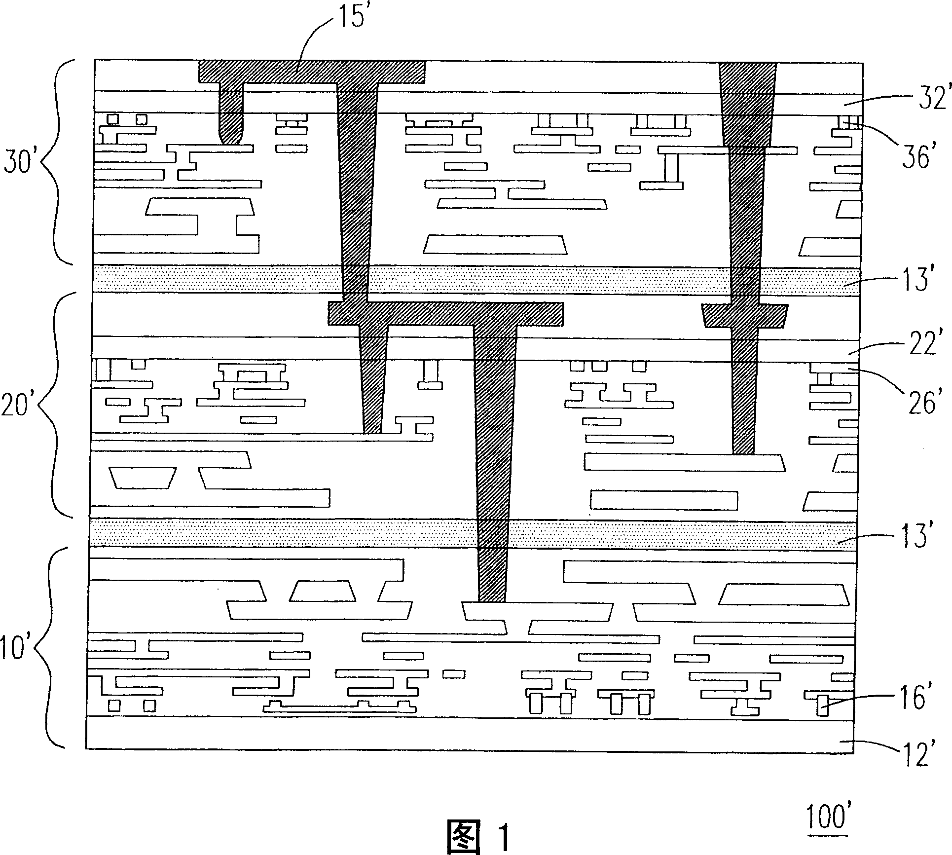
[0063] The three-dimensional wafer stack structure of the present invention uses layer-by-layer deposition or laser drilling to form a metal support structure between two hard surfaces (or substrates) on the wafer to provide support for the structure layer and achieve the purpose of strengthening the low dielectric The purpose of the material layer.

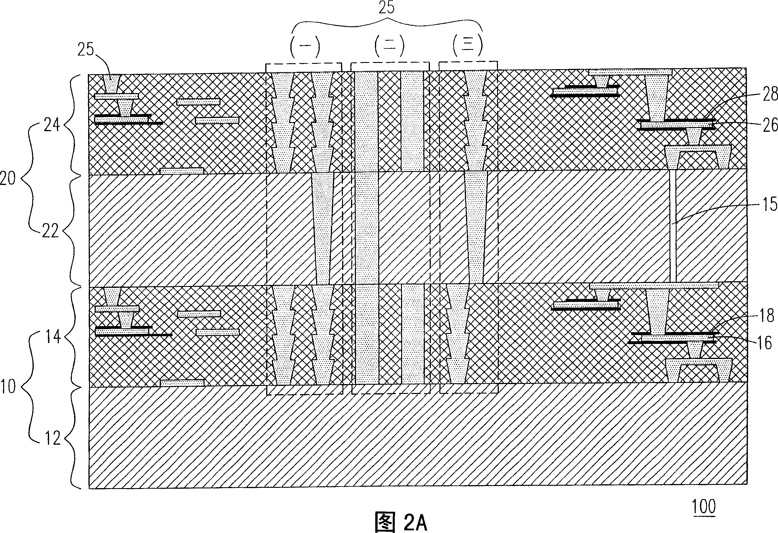
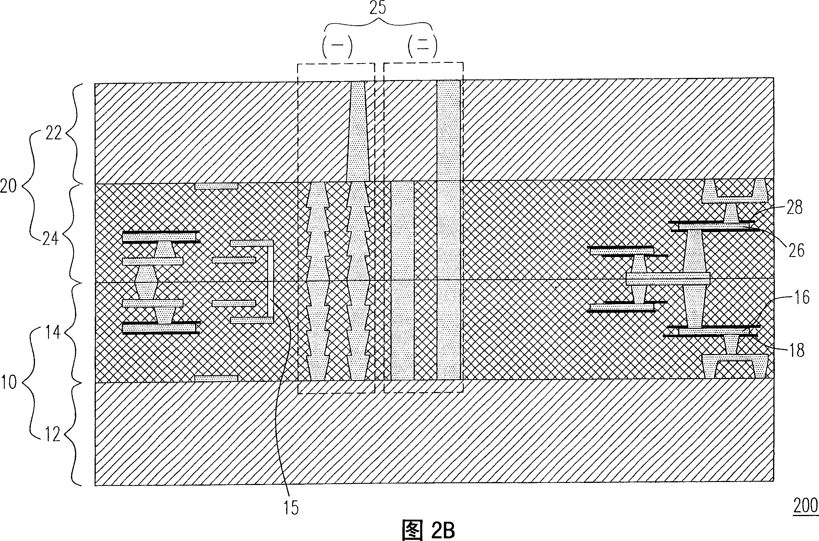
[0064] Please refer to FIGS. 2A-2D , which illustrate various specific embodiments of the three-dimensional wafer stack structure of the present invention. As shown in FIG. 2A, the three-dimensional wafer stack structure 100 of the first embodiment of the present invention is composed of a first wafer 10 and a second wafer 20, wherein the first and second wafers 10, 20 are all facing upwards. (face up) arrangement (or called back to face (back to face or back to front) stacked structure), wherein, the first and second wafers 10, 20 respectively include a first and second substrate layer 12, 22 and a first and a second device lay...


PUM


Abstract

The provided wafer static structure comprises: the first wafers with multiple metal support structures, and the second wafer on top of the first wafer. Wherein, the said support structure is set on chip position to extend from the silicon surface of the first chip to the second wafer base and form a support force for preventing the damage from vertical stress or shearing stress.

Description

technical field [0001] The invention relates to a three-dimensional wafer stacking structure and a three-dimensional wafer stacking method, in particular to a three-dimensional wafer stacking structure including a metal support structure between two silicon substrates and a three-dimensional wafer stacking method. Background technique [0002] With the development of electronic manufacturing technology, more and more electronic products are developed with portability, high functionality, light weight and small size as their development goals. However, under such a development trend, the functionality of the electronic chips used in electronic products and the circuit devices contained in them will inevitably increase and become more and more complex. Under the demand for miniaturized chip areas, Although the current lithographic process of wafer manufacturing is still evolving to 45nm, 32nm and even smaller sizes; however, in any case, major changes in chip design in the fut...

Claims


Application Information

Patent Timeline
IPC IPC(8): H01L25/00H01L21/50
Inventor 张缉熙谭瑞敏廖锡卿骆韦仲李荣贤
Owner IND TECH RES INST
Why Eureka
Try Eureka