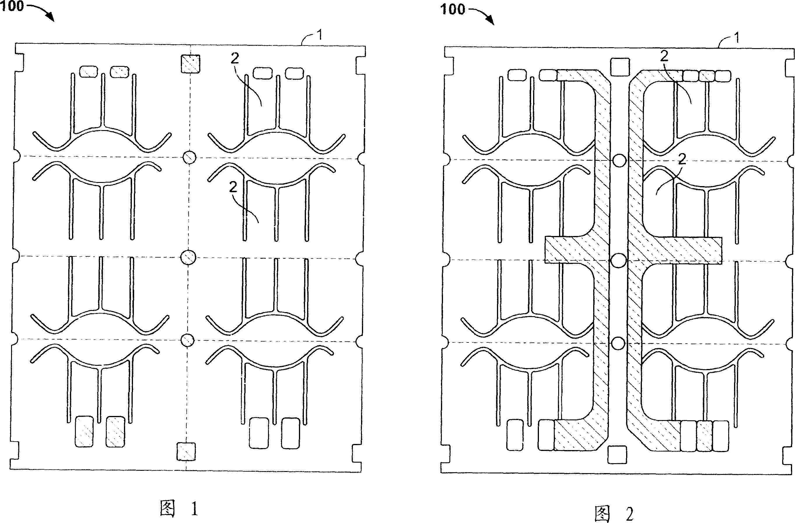
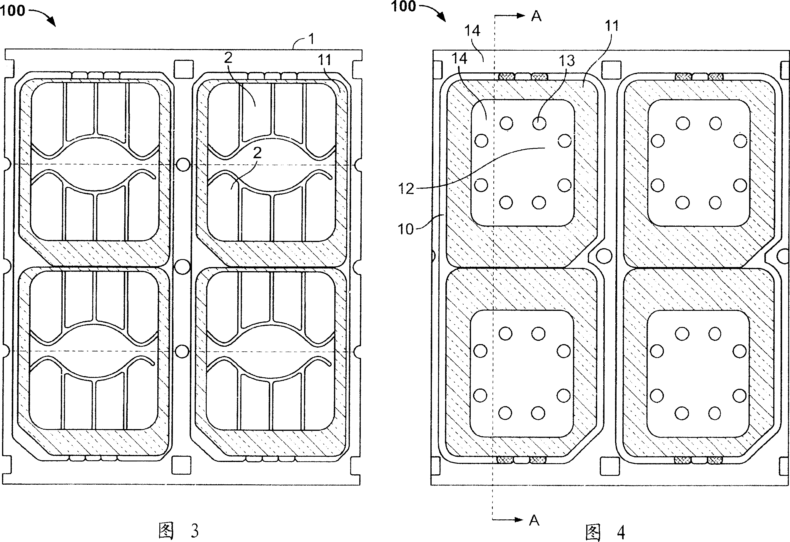
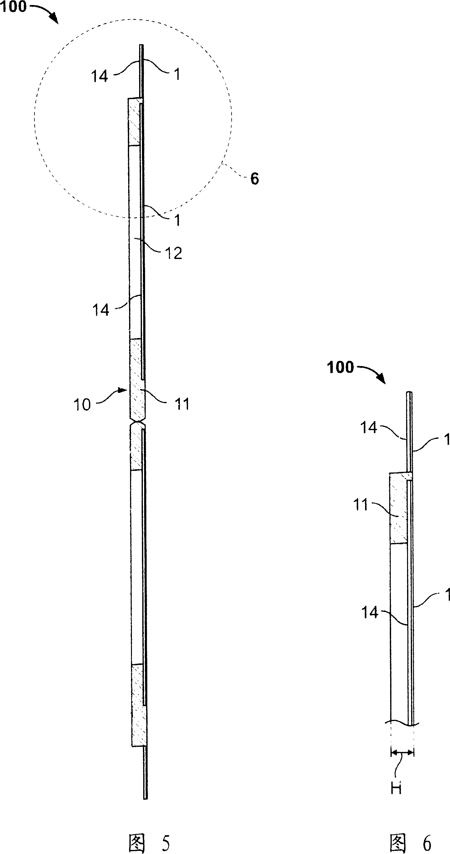
[0031] Figures 1, 2 and 3 show top views of the first surface of the carrier tape. Figure 4 shows a top view of the second surface opposite the first surface. Therefore, Figures 1, 2 and 3 and Figure 4 show top views of both sides of the smart card body according to the present invention.
[0032] It can be seen from FIG. 1 that a large number of smart card bodies 10 are manufactured on the carrier tape 100. The carrier tape 100 is formed of a conductive layer 1 preferably composed of a copper sheet. However, other conductive materials, such as aluminum, can also be used. The carrier tape 100 is preferably composed of a roll of conductive layer 1, so that a large number of smart card main bodies 10 can be manufactured using the roll-to-roll method.
[0033] The manufacturing method of the smart card main body 10 containing the semiconductor chip will be explained with reference to FIGS. 1, 2 and 3.
[0034] First, the conductive layer 1 is drilled, and a lead frame is formed in the conductive layer 1. On the first surface of the conductive layer 1 as shown in FIG. 1, the lead frame has a first contact 2, and a punching tool is used to perforate the conductive layer 1 along the roll (shown by the black perforation in FIG. 1) . As shown in FIGS. 1, 2 and 3, two smart card bodies 10 are manufactured in a single web of the conductive roll. Of course, it is also possible to choose to manufacture different numbers of smart card bodies within the width of the roll.
[0035] Once the penetration of the conductive layer 1 is completed and the lead frame is formed, the contacts 2 arranged on the first surface are metalized. The first contact 2 is preferably coated with nickel and nickel-phosphorus by an electroplating process. However, other metallization processes, such as sputtering, vapor deposition or the like, can also be used for the penetrated conductive layer 1. The second surface of the conductive layer 1 (not shown in FIGS. 1, 2 and 3) is provided with a second contact 13 preferably composed of gold. These second contacts 13 are used to connect the semiconductor chip to the semiconductor chip to be combined with the first contact 2 of the lead frame. The semiconductor chip is preferably connected to the second contact 13 by wire bonding.
[0036]Afterwards, a pre-perforated dielectric layer (not shown in FIGS. 1, 2 and 3) is laminated on the second surface of the conductive layer 1. The adopted method of pre-drilling the dielectric layer makes the second contact 13 correspond to the perforation of the dielectric layer.
[0037] Afterwards, the dielectric layer is activated by laser treatment, wherein the laser treatment increases the surface roughness of the dielectric layer. This processing step is necessary, and its purpose is to ensure that the injection molded plastic material coated in the subsequent processing steps adheres to the surface of the dielectric layer.
[0038] It can be seen from FIG. 2 that the perforating punch punches the carrier tape 100 (as shown by the black perforated holes), thereby forming the form of the smart card main body 10.
[0039] According to an advantageous embodiment of the present invention, as shown in FIG. 2, two smart card bodies 10 are manufactured in a single web of a roll, the punching tool pierces the first half of each of the two first smart card bodies, and the other punches the first half of each of the two first smart card bodies. The hole tool penetrates the second half of each of the two second smart card bodies. Therefore, the movement along the roll allows the two halves of the smart card body to be penetrated within one width of the roll and to build the outline of the smart card body.
[0040] It can be seen from FIG. 3 that the shell layer 11 is formed on the second surface of the smart card main body by insulating injection molding material. Here, the plastic material is injection-molded around the laminated conductive layer 1. The injection molded shell layer 11 thus forms edges on all sides of the smart card body 10 around both the first and second contacts 2 and 13, and the smart card body 10 thus formed preferably corresponds to the specifications of the 3FF smart card.
[0041] FIG. 4 shows a top view of the second surface of the smart card main body 10, and FIG. 5 shows a cross-section through the carrier tape 100 taken along the A-A section line shown in FIG. 4. Fig. 6 is an enlarged view of the detail VI of the cross section shown in Fig. 5.
[0042] It can be seen from FIG. 4 that the housing layer 11 has a recess 12 for accommodating a semiconductor chip. The second contact 13 is arranged on the conductive layer 1 and the dielectric layer 14 laminated on the conductive layer 1 is pre-drilled in a manner that makes the second contact 13 easy to contact with the semiconductor chip to be bonded.
[0043] It can be seen from FIGS. 5 and 6 that the combined height of the shell layer 11 and the surface layer (not shown in the figure) laminated on the shell layer 11 in the subsequent processing steps of assembling the smart card corresponds to the thickness of the smart card according to the 3FF specification . The height of the outer shell layer 11 preferably has a value H of 0.7 mm, and the thickness of the laminated surface layer has a value of 0.1 mm. It can be seen from FIG. 6 that the height H of the outer shell layer 11 includes the first surface of the injection molding material arranged in the same plane as the first surface of the conductive layer 1 and the first surface of the injection molding material on which the surface layer is to be laminated. The distance between the second surfaces.
[0044] The assembly of the smart card will be described in more detail below.
[0045] The semiconductor chip is embedded in the recess 12 of the shell layer 11 of the smart card main body 10. Preferably, the semiconductor chip is bonded to the dielectric layer 14. Alternatively, the semiconductor chip may be directly fixed to the conductive layer 1. After that, the recess 12 provided with the semiconductor chip in the outer shell 11 of the smart card main body 10 is sealed. Preferably, the carrier tape is laminated to the recess 12 in the outer shell layer 11.
[0046] According to an advantageous embodiment of the present invention, a large number of smart card bodies 10 are manufactured on the carrier tape 100 using the roll-to-roll method. In this way, the carrier tape can be provided to the smart card manufacturer, who only needs to perform the processing steps including the mounting of the semiconductor chip and the sealing of the casing layer 11, thereby simplifying the manufacturing method of the smart card. Since the large number of smart card bodies 10 can be detached from the carrier tape 100, it is only necessary to separate the smart cards after assembly.
[0047] The manufacturing method of the smart card main body according to the present invention realizes a more flexible and simple manufacturing of a Subscriber Identity Module (SIM) card. The smart card main body 10 can be manufactured on the carrier tape 100 using the roll-to-roll method. Next, the carrier tape 100 can be provided to a smart card manufacturer who only needs to install a semiconductor chip and close the smart card main body, thereby manufacturing the smart card.