ESD protection element
An ESD protection and component technology, applied in electrical components, electrical solid-state devices, semiconductor devices, etc., can solve the problem of not being able to form a high-pass filter into one chip, etc.
- Summary
- Abstract
- Description
- Claims
- Application Information
AI Technical Summary
Problems solved by technology
Method used
Image

Examples
Embodiment 1
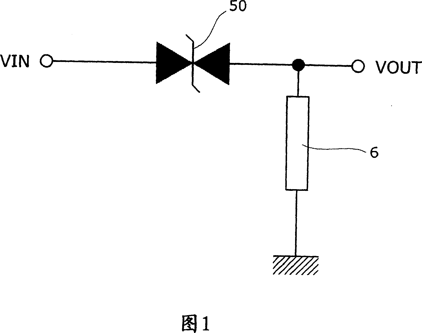
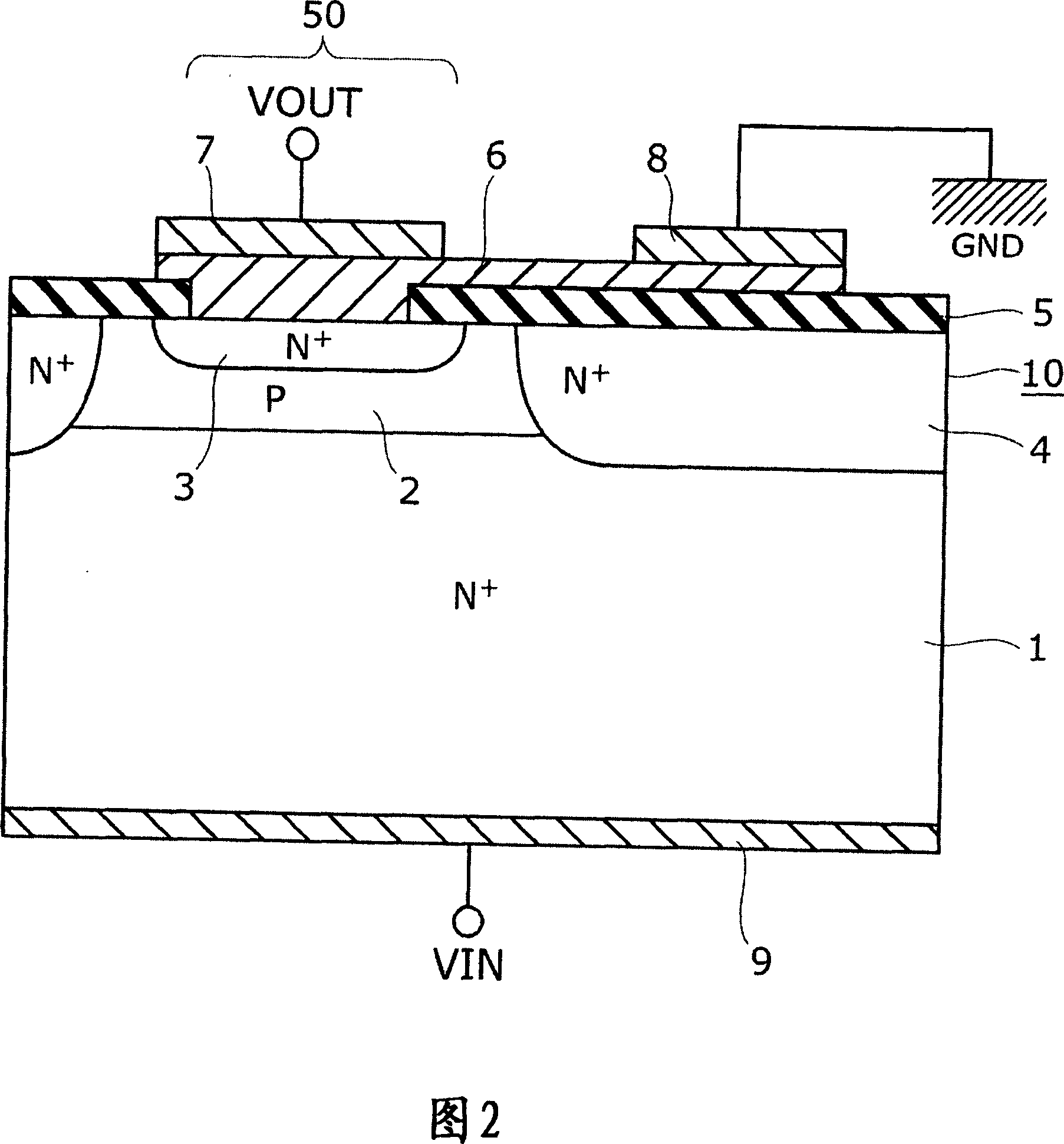
[0048] Embodiment 1 will be described with reference to FIG. 1 and FIG. 2 .
[0049] FIG. 1 is an equivalent circuit diagram of the ESD protection element of this embodiment, and FIG. 2 is a cross-sectional view of main parts of the ESD protection element of this embodiment. As shown in FIG. 1 , a diode (bidirectional Zener diode) 50 and a resistor 6 constituting an ESD protection element are connected between a signal input (VIN) and a signal output (VOUT). One end of the resistor 6 is connected to one end of the diode 50, and the other end is grounded (GND).
[0050] As shown in FIG. 2, the silicon semiconductor substrate 10 is made of N + Type high-concentration layer 1 and P-type silicon epitaxial layer 2 formed on high-concentration layer 1 . The impurity concentration of the high-concentration layer 1 is greater than or equal to 1×10 19 / cm 3 , the impurity concentration of P-type silicon epitaxial layer 2 is 1×10 15 ~1×10 17 / cm 3 about. An input signal electrod...
Embodiment 2
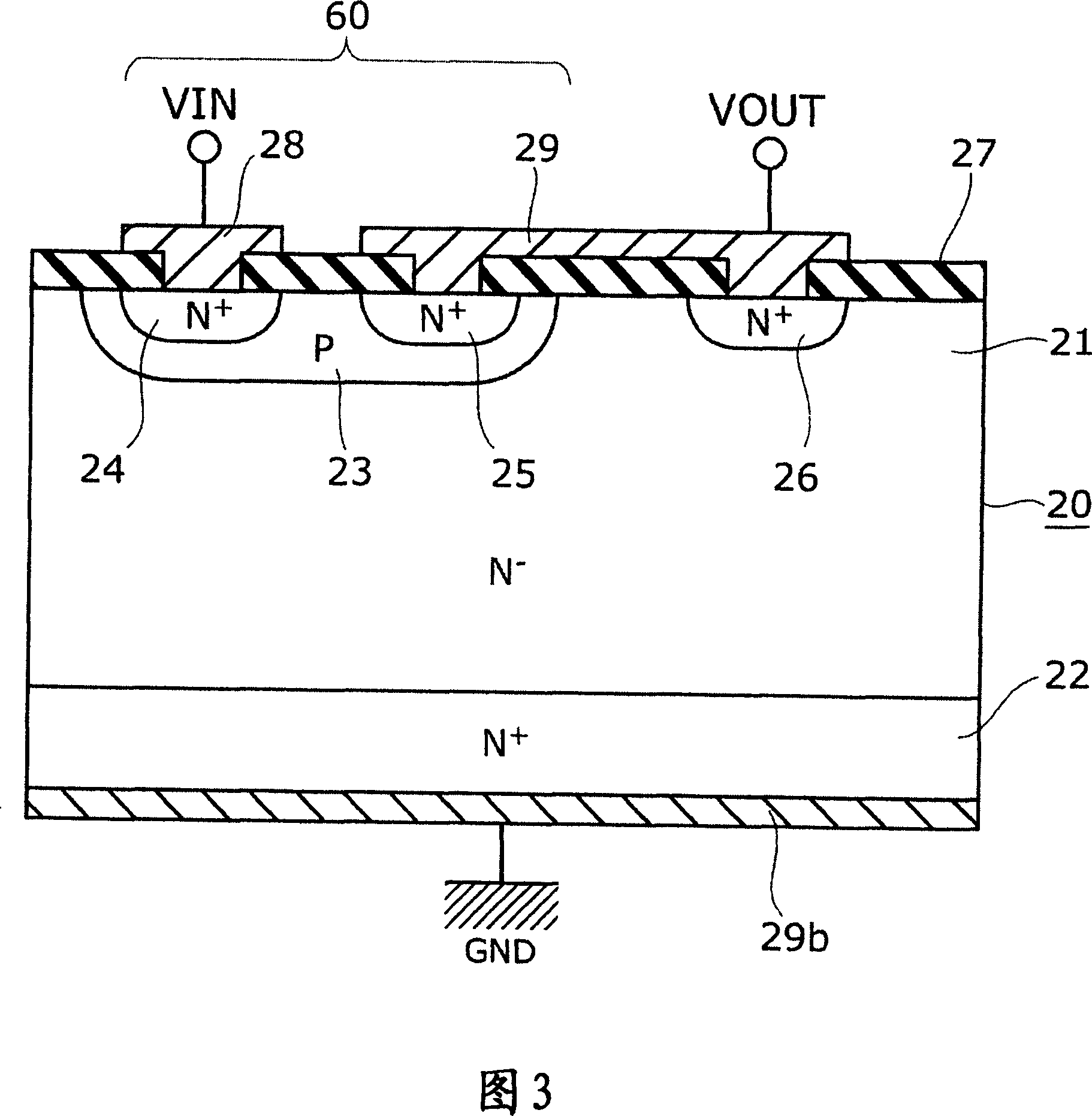
[0055] Next, Embodiment 2 will be described with reference to FIG. 3 .
[0056] FIG. 3 is a cross-sectional view of the ESD protection element of this embodiment. As shown in FIG. 3 , a diode (bidirectional Zener diode) 60 constituting an ESD protection element and an output signal electrode 29 are connected between the signal input (VIN) and the signal output (VOUT). One end of the output signal electrode 29 is connected to one end of the diode 60, and the other end is connected to the N + On the high-concentration impurity diffusion region 26 . The silicon semiconductor substrate 20 is made of N + type high concentration layer 22 and the N formed on the high concentration layer 22 - Silicon epitaxial layer 21 is formed. The impurity concentration of the high concentration layer 22 is greater than or equal to 1×10 19 / cm 3 , N - The impurity concentration of the silicon epitaxial layer 21 is less than or equal to 1×10 14 / cm 3 about. An input signal electrode 28 and...
Embodiment 3
[0064] Next, Embodiment 3 will be described with reference to FIG. 4 .
[0065] FIG. 4 is a cross-sectional view of the ESD protection element of this embodiment. As shown in FIG. 4 , a diode (bidirectional Zener diode) 70 constituting an ESD protection element and an output signal electrode 39 are connected between the signal input (VIN) and the signal output (VOUT). One end of the output signal 39 is connected to one end of the diode 70, and the other end is connected to the N + On the high-concentration impurity diffusion region 36 .
[0066] The silicon semiconductor substrate 30 is made of N + type high concentration layer 32, the N formed on the high concentration layer 32 - Si epitaxial layer 31 and formed on the N - The P-type silicon epitaxial layer 41 on the silicon epitaxial layer 31 is formed. The impurity concentration of the high concentration layer 32 is greater than or equal to 1×10 19 / cm 3 , N - The impurity concentration of the silicon epitaxial laye...
PUM
 Abstract
Description
Claims
Application Information
 - R&D
- Intellectual Property
- Life Sciences
- Materials
- Tech Scout
- Unparalleled Data Quality
- Higher Quality Content
- 60% Fewer Hallucinations
Browse by: Latest US Patents, China's latest patents, Technical Efficacy Thesaurus, Application Domain, Technology Topic, Popular Technical Reports.
© 2025 PatSnap. All rights reserved.Legal|Privacy policy|Modern Slavery Act Transparency Statement|Sitemap|About US| Contact US: help@patsnap.com