Method for adopting positive electronic corrosion-resistant to prepare metal nano electrode

A metal nano-resist technology, applied in circuits, electrical components, opto-mechanical equipment, etc., can solve the problems of single electrode material, low efficiency, and difficult optical lithography resolution to reach nanoscale resolution.

Active Publication Date: 2007-06-13
SEMICON MFG INT (SHANGHAI) CORP +1
View PDF3 Cites 9 Cited by
  • Summary
  • Abstract
  • Description
  • Claims
  • Application Information

AI Technical Summary

Problems solved by technology

The Chinese invention patent with application number 200410010181.2 uses an atomic force microscope (AFM) to etch nanowires combined with chemical methods to prepare silver nanoelectrodes, which has the disadvantages of low efficiency and incapable of large-scale production
The Chinese invention patent with application number 99116576.4 uses flame melting and etch...

Method used


Image

  • Method for adopting positive electronic corrosion-resistant to prepare metal nano electrode
  • Method for adopting positive electronic corrosion-resistant to prepare metal nano electrode

Examples


specific Embodiment

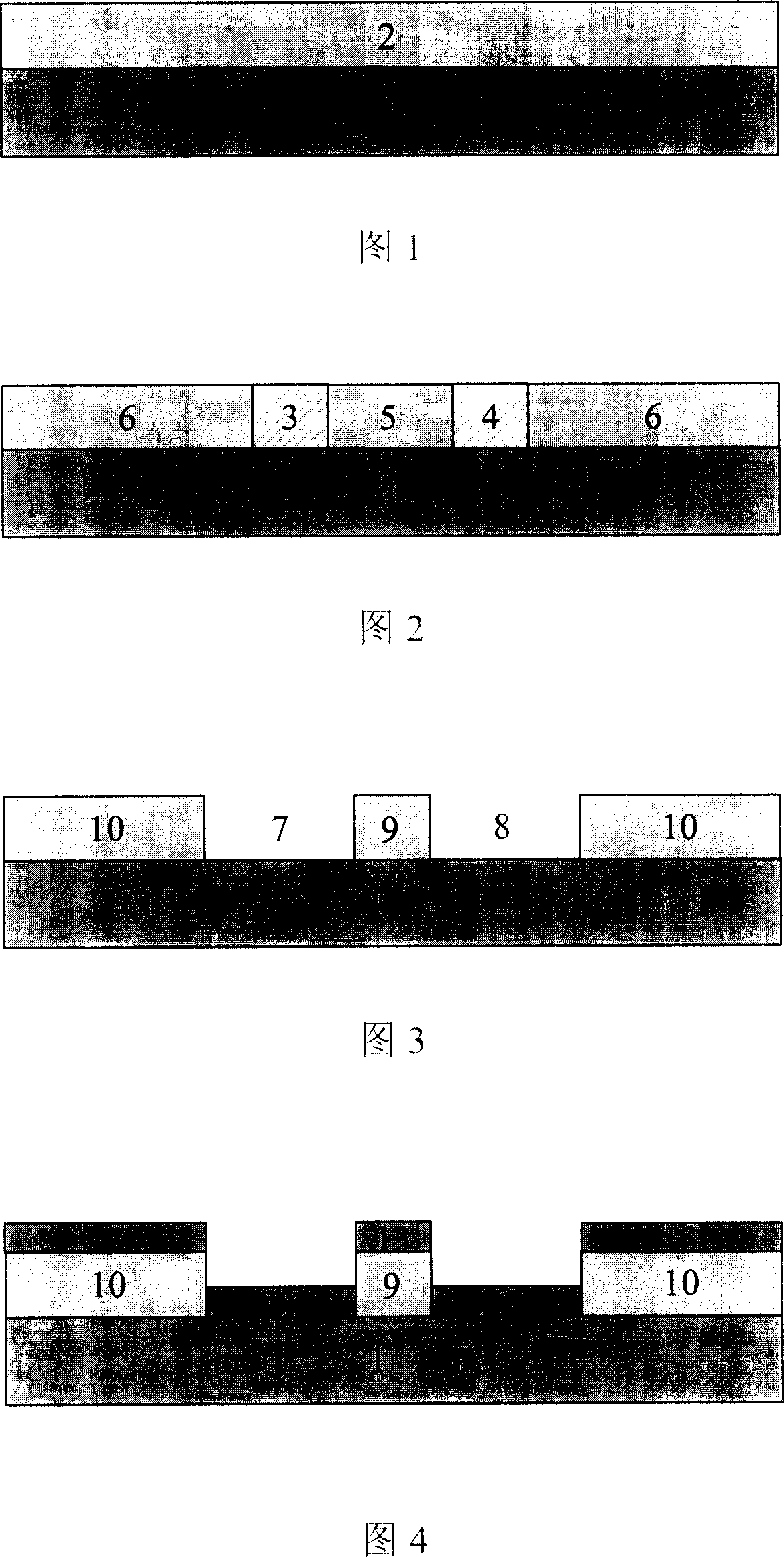
[0027] Taking the use of ZEP520 positive electronic resist and evaporating Cr / Au double-layer metal electrode film as an example, the detailed process and steps of the present invention are further described in conjunction with the accompanying drawings, wherein:

[0028] As shown in Figure 1, the surface is flat and clean with SiO 2 On the Si substrate 1 of the insulating film, a single-layer ZEP520 positive electronic resist 2 was coated with a coater, the coating speed was 2000 rpm, the coating time was 60 seconds, and the thickness of the resist was 485 nm. Then use an oven to pre-bake at 180°C for 20 minutes.

[0029] As shown in Figure 2, the electron beam direct writing exposure was performed on the regions 3 and 4 of the ZEP520 resist 2, and the regions 5 and 6 were not exposed. The width of the region 3 and the region 4 is 350 nm, and the interval between the region 3 and the region 4, that is, the width of the unexposed region 5 is 250 nm. Electron beam exposure ca...


PUM


Abstract

A method uses the positive electron anticorrosion agent to prepare metal nano electrode. The main features of the invention is to use the neighboring effect of electron band, use the EBL to gain a pair or a group of the positive electron anticorrosion agent groove figures that have line, hole and other various shapes at the space that is measured by nano on various underlay, and then use secondly the metal deposition and peel off technology to prepare various metal material nano electrode. The main procedures of which include coating the positive electron anticorrosion agent on the interlay; baking frontally; expose by direct electron band; develop; to fix; vaporize or sputtering metal; to peel off in the acetone. The distance between the metal nano electrode that is prepared by such method can be 30~100mm, is suitable to make various quanta component, nano line, nano tube component, single electronic component and various components or circuit. The method has many advantages, such as: less technology procedure, simple, stable and reliable, multiple uses and can be compatible with the traditional CMOS technology.

Description

technical field [0001] The invention belongs to the technical field of nano processing, in particular to a method for preparing a metal nano electrode. Background technique [0002] For more than half a century, semiconductor integrated circuits with CMOS as the mainstream technology have been developing rapidly following "Moore's Law". Nanoelectronic devices with new principles, such as various quantum dot devices, nanowires, nanotube devices, and single-electron devices, have become research hotspots. In the manufacture of these nanoelectronic devices, the manufacture of nanoelectrodes with small size, good conductivity and nanoscale gaps is a key and difficult point. [0003] The Chinese invention patent with application number 200410095163.9 mainly uses chemical methods combined with the use of polymer materials to prepare electrodes, but this electrode has not reached the nanometer scale. The Chinese invention patent with the application number 200410010181.2 uses an ...

Claims


Application Information

Patent Timeline
IPC IPC(8): H01L21/28H01L21/027G03F7/00
Inventor 龙世兵刘明陈宝钦
Owner SEMICON MFG INT (SHANGHAI) CORP
Why Eureka
Try Eureka