Electronic circuit device
A technology of electronic circuits and analog circuits, applied in logic circuits, electrical components, electrical signal transmission systems, etc., can solve problems such as excessive margin, characteristic deviation, excess current consumption, etc., and achieve reduced power consumption, circuit scale, and accuracy Improves the effect of reducing and suppressing current consumption
- Summary
- Abstract
- Description
- Claims
- Application Information
AI Technical Summary
Problems solved by technology
Method used
Image

Examples
Embodiment 1
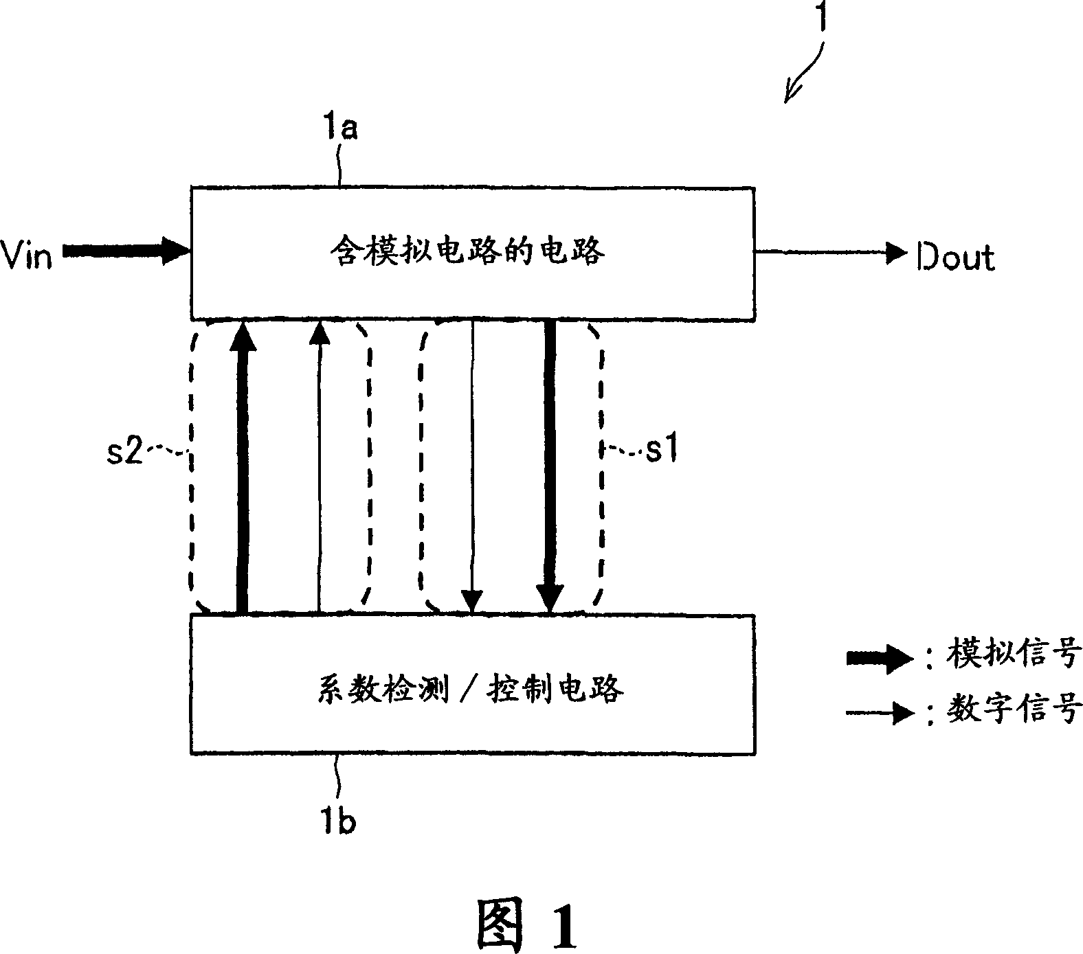
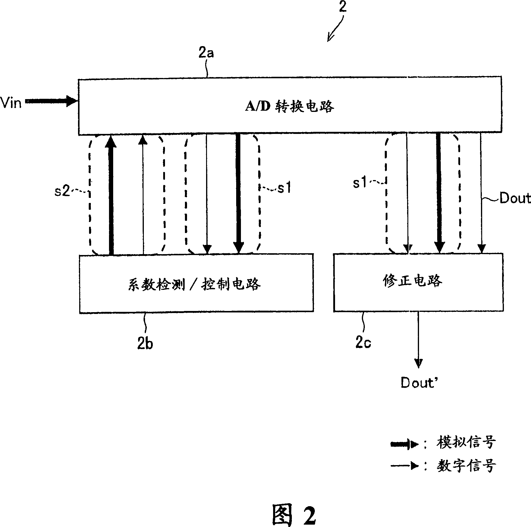
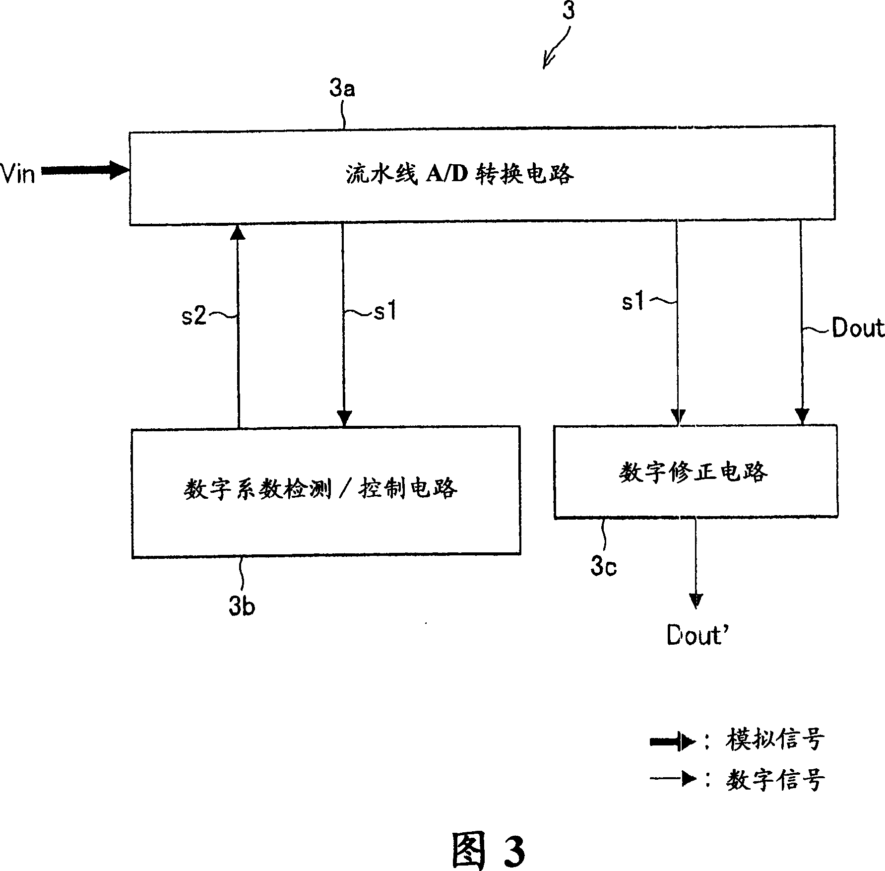
[0096] FIG. 1 is a conceptual diagram of a circuit 1 (electronic circuit device) provided with an analog circuit according to the present invention. The circuit 1 provided with an analog circuit is provided with a circuit 1a including an analog circuit and a coefficient detection / control circuit 1b. Circuit 1a comprising analog circuits processes an analog input signal Vin. The processed result is output, for example the digital output Dout shown in the figure. In addition, the circuit 1a including an analog circuit outputs a coefficient s1 representing a predetermined characteristic of the analog circuit, and inputs it to a coefficient detection / control circuit 1b.
[0097] As the predetermined characteristics, voltage and current at predetermined positions of the above-mentioned analog circuit, and numerical values expressed by them, etc. may be mentioned. If a predetermined characteristic can be detected when the analog circuit is manufactured, the manufacturing variati...
Embodiment 2
[0160] FIG. 9 shows the configuration of a circuit (electronic circuit device) 5 provided with an A / D conversion circuit in this embodiment. The circuit 5 provided with the A / D conversion circuit constitutes a modified A / D conversion circuit, and the A / D conversion circuit of Embodiment 1 is provided at all stages of the first stage to the N-1th stage of the pipeline A / D conversion circuit 4a. The bias voltage generating circuit 4d of the circuit 4 (see FIG. 4 ) of the D conversion circuit. Therefore, it is possible to set the optimum bias voltage Vb for each stage. Hereinafter, each bias voltage generating circuit is referred to as 5dk (k=1 to N).
[0161] In the control method when bias voltage generating circuits are provided for all stages from the 1st stage to the N-1st stage, each stage can be set individually in random order, but if the flow chart shown in Fig. 10 is used to set , the efficiency is better.
[0162]Generally, in the modified A / D conversion circuit, th...
PUM
 Abstract
Description
Claims
Application Information
 - R&D
- Intellectual Property
- Life Sciences
- Materials
- Tech Scout
- Unparalleled Data Quality
- Higher Quality Content
- 60% Fewer Hallucinations
Browse by: Latest US Patents, China's latest patents, Technical Efficacy Thesaurus, Application Domain, Technology Topic, Popular Technical Reports.
© 2025 PatSnap. All rights reserved.Legal|Privacy policy|Modern Slavery Act Transparency Statement|Sitemap|About US| Contact US: help@patsnap.com