Three dimensional thin film transistor nanocrystal memory element and producing method thereof

A technology for memory elements and thin film transistors, which is applied in the manufacture of semiconductor/solid-state devices, electric solid-state devices, semiconductor devices, etc., can solve the problems of difficult process, high deposition temperature, and low density of a single layer of three-dimensional memory, etc. The effect of process temperature

Inactive Publication Date: 2007-07-04
IND TECH RES INST
View PDF0 Cites 0 Cited by
  • Summary
  • Abstract
  • Description
  • Claims
  • Application Information

AI Technical Summary

Problems solved by technology

Three-dimensional memory means that there are multiple layers of storage elements on the substrate. It is not necessary to make all the storage cells on a single layer of the substrate, and the storage cells can also be stacked vertically. However, the manufacturing process has certain complexity and difficulty.
[0006] However, although thin-film transistors can be used to reduce its process temperature, the dielectric layer ONO, which is the core of the memory structure using SONOS, still requires a relatively high deposition temperature. Cause damage, making it difficult to process
In addition, the bit density of a single layer of this structure to make a three-dimensional memory is not high

Method used


Image

  • Three dimensional thin film transistor nanocrystal memory element and producing method thereof
  • Three dimensional thin film transistor nanocrystal memory element and producing method thereof
  • Three dimensional thin film transistor nanocrystal memory element and producing method thereof

Examples


Embodiment

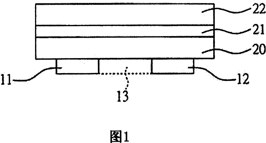
[0032] The structure, manufacturing method and operation method of the three-dimensional stacked thin film transistor nano-grain memory element of the present invention will be described in detail below with reference to the accompanying drawings.

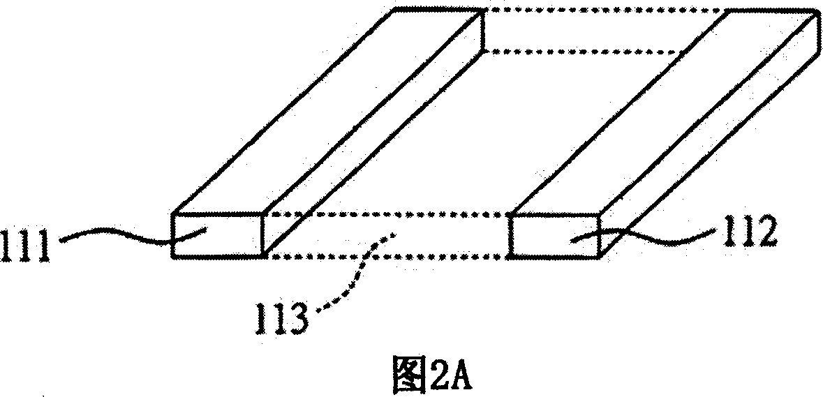
[0033] 2A to FIG. 2G are diagrams illustrating the fabrication method of the three-dimensional stacked TFT-type nano-grain memory device of the present invention.

[0034]As shown in Figure 2A, at first, a first doped polysilicon layer is grown on the silicon substrate, and the bit line patterns 111 and 112 are defined by methods such as coating photoresist, exposure and etching in the prior art, and then the bit line patterns 111 and 112 are defined. An oxide layer 113 is filled between the lines, and then planarized by a suitable method such as chemical mechanical polishing (CMP).

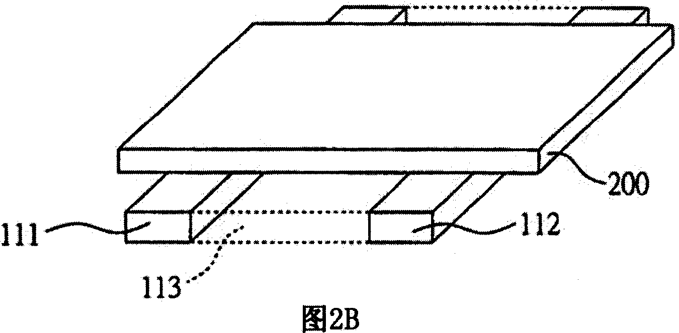
[0035] Furthermore, as shown in FIG. 2B, on the bit lines 111, 112 and the oxide layer 113, a second doped polysilicon layer 200 with opposite polari...


PUM


Abstract

The invention discloses a 3D thin film transistor nanocrystalline memory component and its manufacturing method, the memory component includes: a thin film transistor formed in the substrate; a nanocrystalline layer in the thin film transistor gate dielectric layer; the other thin film transistor formed in the thin film transistor; these two thin film transistors share one character line. This invention provides a production method of lower memory components manufacturing temperature, and when stacking in the vertical direction, each memory components can not have different memory components characteristics in each layers by the different thermal budget of each layer, and when the 3D memory of the invention stacks memory components of each layer, no need to additional solve the on-line problem of each layer's memory components extending outward to the substrate transistors, that is to say, it provides an active memory components to stack vertically the memory components, and furthermore, the invention can enhance 3D memory bit density and simplify the manufacturing complexity.

Description

technical field [0001] The invention relates to a structure of a semiconductor element and a manufacturing method thereof, in particular to a structure and a manufacturing method of a thin film transistor type nano crystal grain memory element. Background technique [0002] Due to the popularization of electronic products and computer-related products, the demand for semiconductor storage devices has increased rapidly. Therefore, in recent years, one research and development focus of the semiconductor memory manufacturing process is how to configure and stack the three-dimensional memory of multi-layer memory cells on the substrate. Three-dimensional memory means that there are multiple layers of storage elements on the substrate. It is not necessary for all storage units to be located on a single layer of the substrate, and the storage units can also be stacked vertically. However, the manufacturing process has certain complexity and difficulty. [0003] With the existing ...

Claims


Application Information

Patent Timeline
Patent Type & Authority Applications(China)
IPC IPC(8): H01L21/8239H01L27/105
Inventor 郑培仁
Owner IND TECH RES INST
Why Eureka
Try Eureka