Supercharge Your Innovation With Domain-Expert AI Agents!

Image sensor and method of manufacturing the same

A technology of image sensor and manufacturing method, applied in semiconductor/solid-state device manufacturing, electric solid-state device, semiconductor device, etc., can solve the problems of long focal length, crosstalk, and reduced sensitivity, etc.

Inactive Publication Date: 2007-07-04
DONGBU ELECTRONICS CO LTD
View PDF0 Cites 5 Cited by
  • Summary
  • Abstract
  • Description
  • Claims
  • Application Information

AI Technical Summary

Problems solved by technology

Therefore, the focal distance from the microlens 114 to the photodiode area becomes longer, causing crosstalk between adjacent pixels and reducing sensitivity

Method used


Image

  • Image sensor and method of manufacturing the same
  • Image sensor and method of manufacturing the same
  • Image sensor and method of manufacturing the same

Examples


Embodiment Construction

[0049] Hereinafter, a CMOS image sensor and a manufacturing method thereof according to preferred embodiments of the present invention will be described in detail with reference to the accompanying drawings.

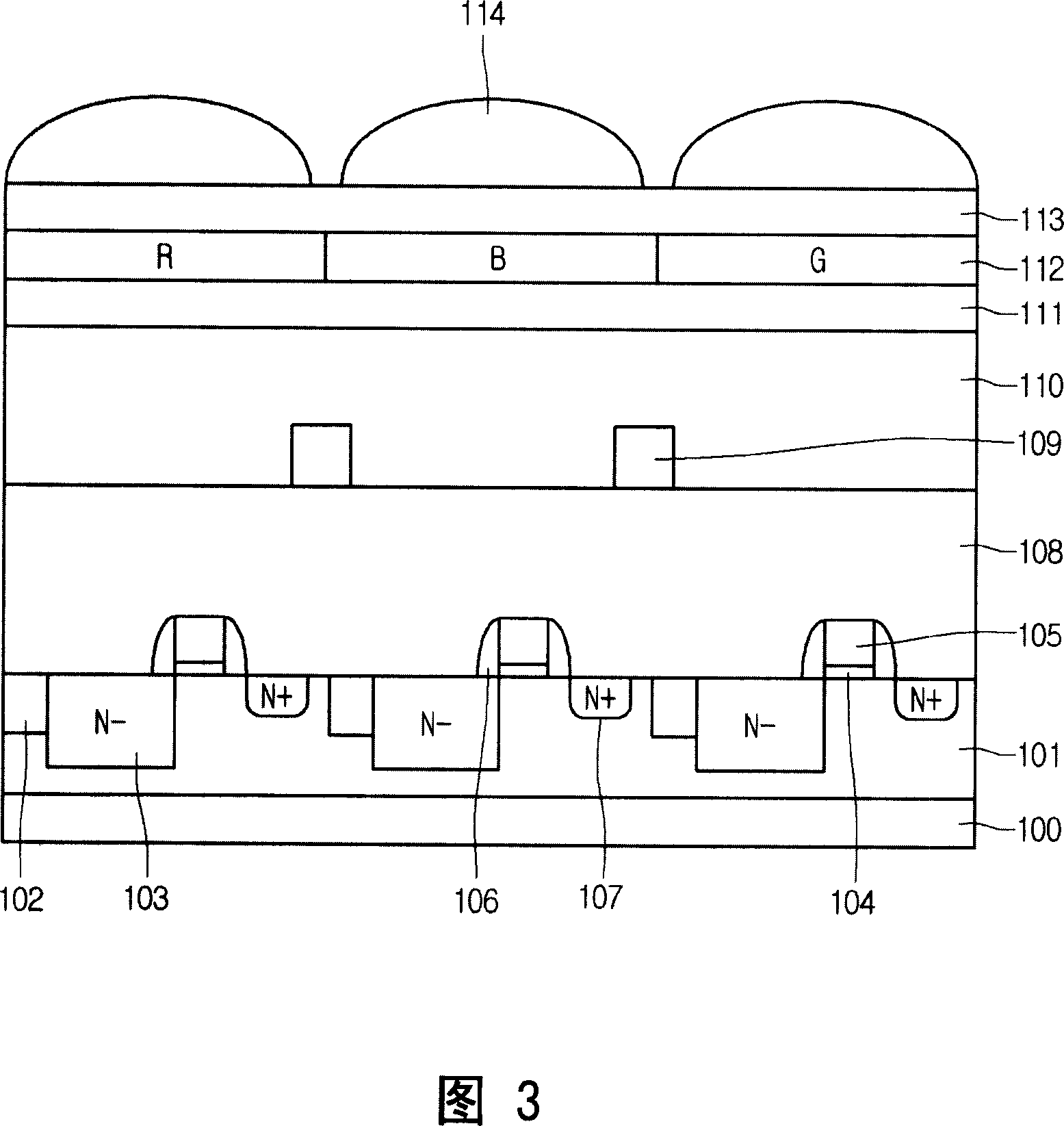
[0050] 4 is a cross-sectional view of a CMOS image sensor according to the present invention.

[0051] Referring to FIG. 4, at P defining isolation regions and active regions (photodiode regions and transistor regions) ++ P-type semiconductor substrate 200 grows P - A type epitaxial layer 201 is formed, and a field oxide layer 202 for separating the input regions of green light, red light and blue light is formed in the isolation region of the semiconductor substrate 200 . The gate electrode 204 is formed by inserting the gate insulating layer 203 in the active region of the semiconductor substrate 200 .

[0052] In addition, n is formed in the photodiode region of the semiconductor substrate 200 - Type diffusion regions 205 are formed, and sidewall insulating layers ...


PUM


Abstract

A CMOS image sensor and a method of manufacturing the same are provided. The CMOS image sensor includes a semiconductor substrate including a plurality of photodiodes and a plurality of transistors, a first interlayer dielectric formed on the semiconductor substrate, a metal wiring and a second interlayer dielectric formed on the first interlayer dielectric, a plurality of color filter layers formed in the trenches formed in the second interlayer dielectric, and a plurality of micro lenses formed on the plurality of the color filter layers.

Description

technical field [0001] The present invention relates to a CMOS image sensor and a manufacturing method thereof. Background technique [0002] Image sensors are semiconductor devices used to convert optical images into electrical signals. A CCD (Charge Coupled Device) is a semiconductor device in which MOS (Metal Oxide Semiconductor) capacitors are located very close to each other and charge carriers are transferred to or stored in the capacitors. [0003] Meanwhile, the CMOS image sensor is a device using a switch mode that sequentially detects outputs by providing MOS transistors corresponding to the number of pixels by CMOS technology using peripheral devices such as a control circuit and a signal processing circuit. [0004] However, a CCD (Charge Coupled Device) has a complicated driving method, high power consumption, and requires a multi-step mask process, so its manufacturing process is complicated. In addition, the signal processing circuit cannot be implemented in...

Claims


Application Information

Patent Timeline
Patent Type & Authority Applications(China)
IPC IPC(8): H01L27/146H01L21/822
CPCH01L27/14621H01L27/14685H01L27/14627H01L27/14645H01L27/14689H01L27/146
Inventor 玄佑硕
Owner DONGBU ELECTRONICS CO LTD
Features
  • R&D
  • Intellectual Property
  • Life Sciences
  • Materials
  • Tech Scout
  • Unparalleled Data Quality
  • Higher Quality Content
  • 60% Fewer Hallucinations
Learn More