Impurity introducing method
An impurity and plasma technology, applied in the manufacture of discharge tubes, electrical components, semiconductor/solid-state devices, etc., can solve the problems of insufficient precision of shallow amorphous layers and narrow range of annealing conditions.
- Summary
- Abstract
- Description
- Claims
- Application Information
AI Technical Summary
Problems solved by technology
Method used
Image
Examples
Embodiment approach 1
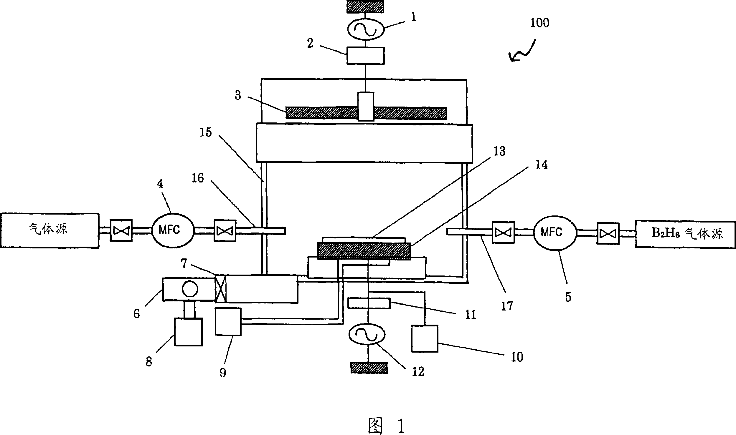
[0138] FIG. 1 is a cross-sectional diagram showing essential parts of an impurity introducing apparatus used in an exemplary embodiment according to the present invention.
[0139] As shown in FIG. 1, the impurity introducing apparatus 100 is configured such that plasma doping, plasma irradiation, and annealing are performed in a sequential manner in the apparatus. Specifically, in the apparatus 100, a semiconductor substrate as the substrate to be processed 13 is provided on a susceptor as the lower electrode 14 placed in the vacuum chamber 15, and a plasma generation region is formed near the surface of the substrate, thereby Perform plasma doping and plasma irradiation. The coil 3 is fixed to a high-frequency power source through the matching box 2 , whereby the high-frequency power source is supplied between the coil 3 and the lower electrode 14 . The lower electrode 14 is connected not only to the DC power source 10 but also to the high frequency power source 12 through ...
Embodiment approach 2
[0149] Hereinafter, a second exemplary embodiment of the present invention will be described.
[0150] Although in the first exemplary embodiment impurities are introduced after the surface of the silicon substrate is formed to be amorphous, the second exemplary embodiment is characterized in that the amorphous layer is formed by irradiating inactive gas phase plasma after introducing impurities .
[0151] In other words, after the degree of vacuum of the vacuum chamber 15 is set, the diborane gas introduction pipe 17 is opened, thereby forming an impurity introduction layer in a predetermined region of the silicon substrate 13 .
[0152] Next, the rare gas introduction pipe 16 is opened to generate rare gas plasma, and the plasma consisting only of electrically inactive particles is irradiated to the silicon substrate 13, thereby forming an amorphous layer. Depending on the conditions of the plasma irradiation, the amorphous layer may or may not have fine pores.
[0153] Af...
Embodiment approach 3
[0156] Hereinafter, a third exemplary embodiment of the present invention will be described.
[0157] Although in the first exemplary embodiment the impurity is introduced after the surface of the silicon substrate is formed to be amorphous, the third exemplary embodiment is characterized in that the impurity introducing step and the irradiation of the inactive gas phase plasma to form the amorphous layer steps.
[0158] In other words, after the vacuum degree of the vacuum chamber 15 is set, the rare gas introduction pipe 16 and the diborane gas introduction pipe 17 are opened together, thereby generating rare gas plasma, and the plasma consisting of only electrically inactive particles The silicon substrate 13 is irradiated, whereby an amorphous layer is formed, and at the same time, an impurity-introducing layer is formed in a predetermined region of the silicon substrate 13 . Depending on the conditions of the plasma irradiation, the amorphous layer may or may not have fi...
PUM
| Property | Measurement | Unit |
|---|---|---|
| diameter | aaaaa | aaaaa |
| depth | aaaaa | aaaaa |
| depth | aaaaa | aaaaa |
Abstract
Description
Claims
Application Information


