CMOS image sensor and fabrication method thereof

a cmos image sensor and image technology, applied in the field of semiconductor device manufacturing, can solve the problems of low transport efficiency, design of pixel units of high-speed cmos image sensors, and inability to transport only signal charges

Active Publication Date: 2018-07-31
SEMICON MFG INT (SHANGHAI) CORP +1
View PDF17 Cites 1 Cited by
  • Summary
  • Abstract
  • Description
  • Claims
  • Application Information

AI Technical Summary

Benefits of technology

[0057]Thus, according to the disclose processes and structures, by the using the disclosed ion implanting scheme, a first implanting region with a second conductive type and a second implanting region with a first conductive type may be formed using a first mask. The second implanting region may be inside of the first implanting region; and may separate the first implanting region into a third implanting region and a fourth implanting region. Then, a fifth implanting region may be formed using a second mask. The fifth implanting region may electrically connect the third implanting region with the fourth implanting region to form a layered diode structure, i.e., a lateral graded-doping profile pinned photodiode (GD-PPD). Such a GD-PPD structure may increase the full well capacity (FWC), the charge transport efficiency (CTE) and the dynamical range the pixel cell of the CMOS image sensor.
[0058]Further, a sixth implanting region may be formed in the CMOS image sensor. The sixth implanting region may be used to adjust the potential barrier balance between the photodiode and the floating diffusion region at the two ends of the transfer transistor. By adjusting the potential barrier balance, the possibly for the charges to reflux back from the floating diffusion region to the photodiode when the transfer transistor is turned on may be reduced; and the image lag may be reduced. Further, because the reflux possibility of the charges may be reduced, the charge transport efficiency (CTE) may be further improved.

Problems solved by technology

Currently, there are certain issues in the design of the pixel units of the high-speed CMOS image sensors.
Thus, the charges of the signal can only be transported by the diffusion of carriers; and the transport efficiency is low.
Second, the image lag phenomenon severely affects the image quality of the CMOS image sensors.
How to avoid the image lag is a big challenge in the design of the high-speed CMOS image sensors.

Method used


Image

  • CMOS image sensor and fabrication method thereof
  • CMOS image sensor and fabrication method thereof
  • CMOS image sensor and fabrication method thereof

Examples


Embodiment Construction

[0013]Reference will now be made in detail to exemplary embodiments of the invention, which are illustrated in the accompanying drawings. Wherever possible, the same reference numbers will be used throughout the drawings to refer to the same or like parts.

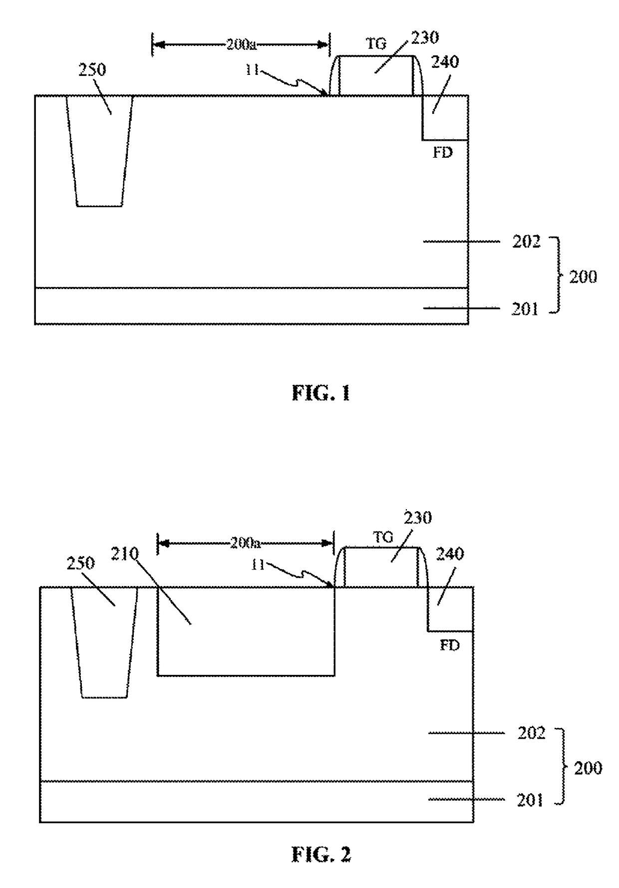
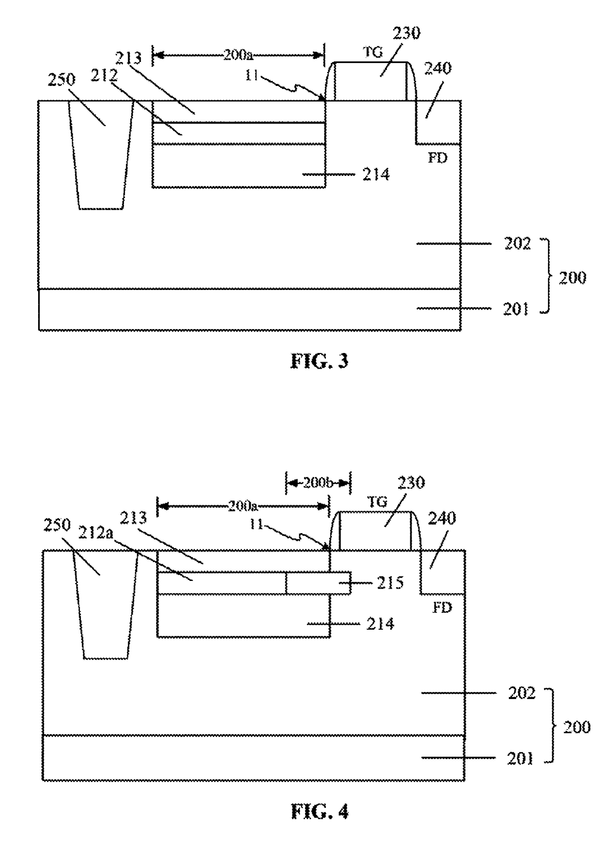
[0014]FIG. 7 illustrates an exemplary fabrication process of a CMOS transistor consistent with the disclosed embodiments; and FIGS. 1-6 illustrate semiconductor structures corresponding to certain stages of the exemplary fabrication process.

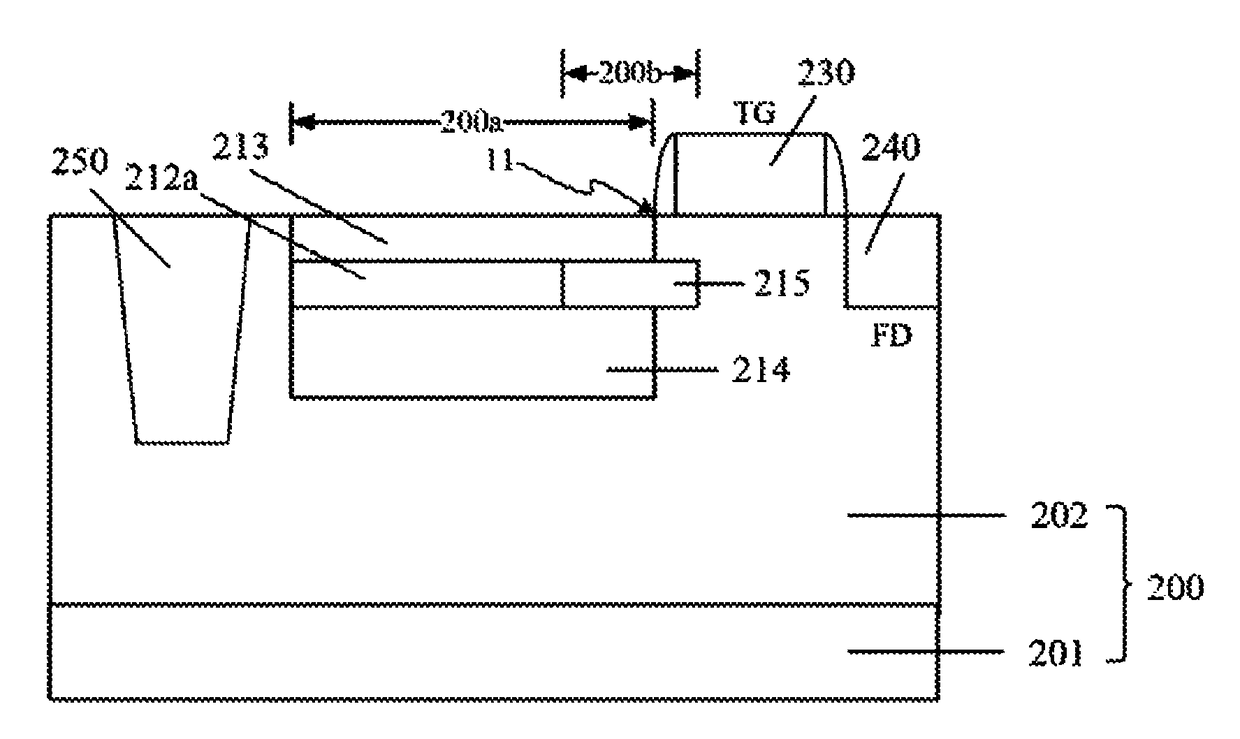
[0015]As shown in FIG. 7, at the beginning of fabrication process, a substrate with certain structures is provided (S101). FIG. 1 illustrates a corresponding semiconductor structure.

[0016]As shown in FIG. 1, a substrate 200 is provided. The substrate 200 may include a base substrate 201 and an epitaxial layer 202. The epitaxial layer 202 is formed on a surface of the base substrate 201.

[0017]The epitaxial layer 202 may have a first conductive type (or doping type). Further, the epitaxial layer 2...


PUM


Abstract

The present disclosure provides CMOS image sensors and fabrication methods thereof. An exemplary fabrication process of a CMOS image sensor includes providing a substrate having a first region and a second region connecting with the first region at a first end of the first region; forming a transfer transistor on surface of the substrate in the second region; forming a first implanting region in the substrate in the first region using a first mask; forming a second implanting region in the first implanting region by, the first implanting region being separated into a third implanting region on the second implanting region and a fourth implanting region under the second implanting region; forming a fifth region in the second region at the first end using a second mask, connecting the third implanting region with the fourth implanting region.

Description

CROSS-REFERENCES TO RELATED APPLICATIONS[0001]This application claims the priority of Chinese patent application No. 201610008022.1 filed on Jan. 7, 2016, the entirety of which is incorporated herein by reference.FIELD OF THE INVENTION[0002]The present invention generally relates to the field of semiconductor manufacturing and, more particularly, related to CMOS image sensors and fabrication processes thereof.BACKGROUND[0003]Image sensors, i.e. photosensitive devices, are apparatus that convert optical images into electrical signals. Image sensors have been widely used in digital cameras and other optical electronic devices. According to the electronic components, image sensors are categorized into two types: Charge Coupled device (CCD) image sensors and Complementary Metal-Oxide semiconductor (CMOS) image sensors (CIS). Comparing with the CCD image sensors, the CMOS image sensors have lower production cost, lower power consumption; and higher integration level, etc. Thus, the CMOS ...

Claims


Application Information

Patent Timeline
Patent Type & Authority Patents(United States)
IPC IPC(8): H01L21/00H01L27/146
CPCH01L27/14612H01L27/1461H01L27/14643H01L27/14689H01L21/266H01L27/14683
Inventor JUNG, DAE-SUBCHEN, DEYANSHI, XUEJIE
Owner SEMICON MFG INT (SHANGHAI) CORP
Why Eureka
Try Eureka