
Method of manufacturing a gallium nitride substrate

a gallium nitride and substrate technology, applied in the direction of polycrystalline material growth, crystal growth process, after-treatment details, etc., can solve the problems of gan substrate breaking, gan substrate breaking, and gan substrate breaking, etc., to achieve low cost, large area, and failure of gan substrate due to silicon nitride layer

Active Publication Date: 2018-10-09
SAMSUNG ELECTRONICS CO LTD
View PDF10 Cites 0 Cited by
  • Summary
  • Abstract
  • Description
  • Claims
  • Application Information

AI Technical Summary

Benefits of technology

This approach allows for the cost-effective manufacturing of large-area GaN substrates with reduced cracks and breakage, maintaining substrate integrity and enabling the production of high-quality, free-standing GaN substrates with a flat surface.

Problems solved by technology

However, a difference between thermal expansion coefficients of sapphire and GaN may be relatively great, so that the GaN substrate formed on the sapphire substrate may be broken during a temperature lowering process.
Due to the silicon nitride layer, the silicon substrate may not be easily removed, and thus, the GaN substrate may be broken.
Thus, failures of the GaN substrate due to the silicon nitride layer, e.g., cracks or a breakage, etc., may decrease.

Method used


Image

  • Method of manufacturing a gallium nitride substrate
  • Method of manufacturing a gallium nitride substrate
  • Method of manufacturing a gallium nitride substrate

Examples


Embodiment Construction

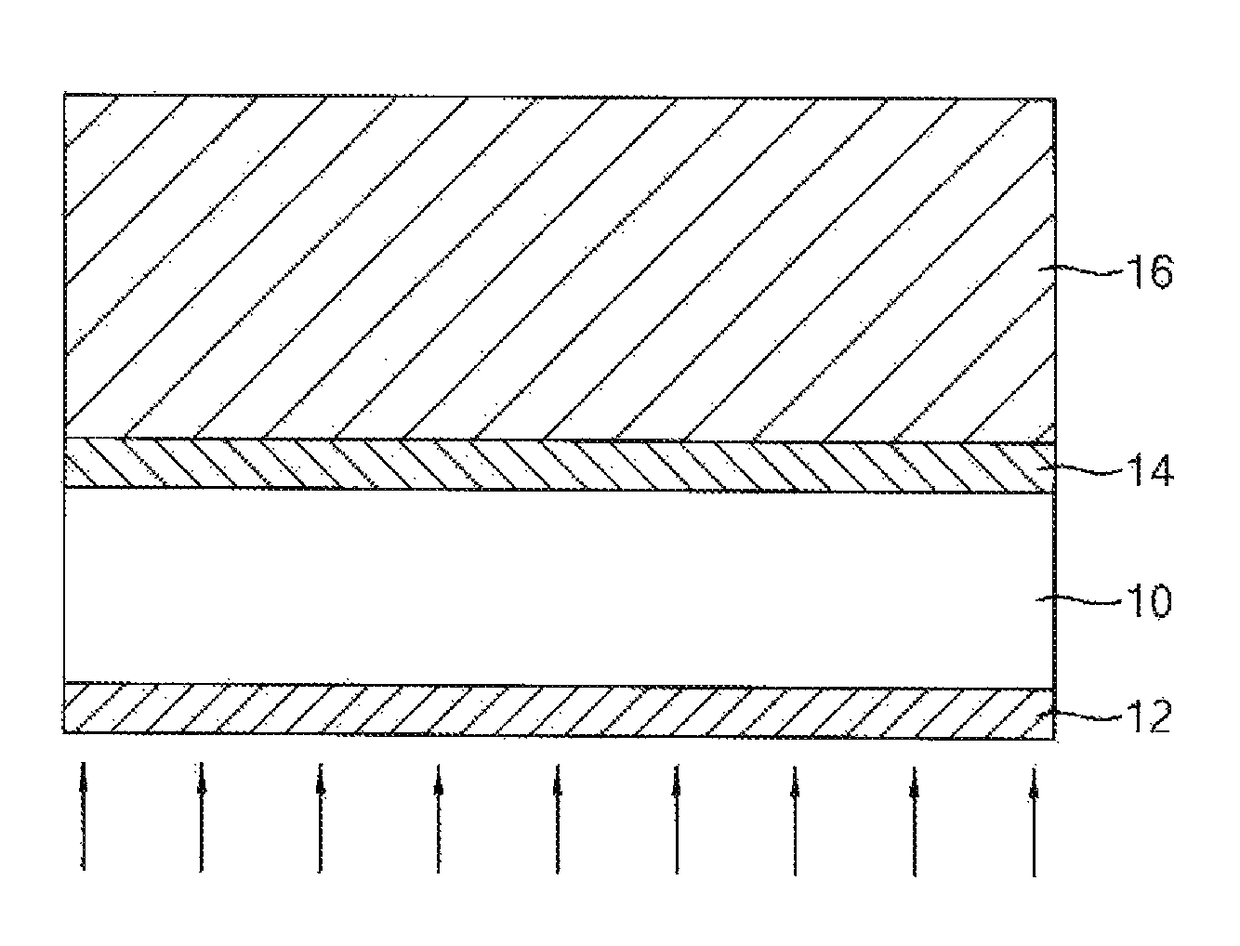
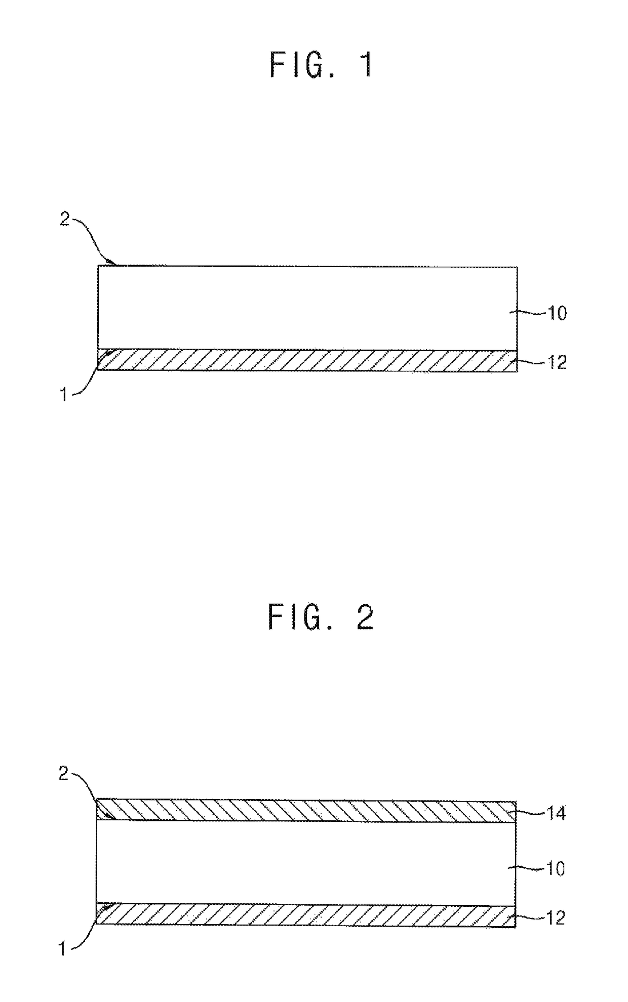
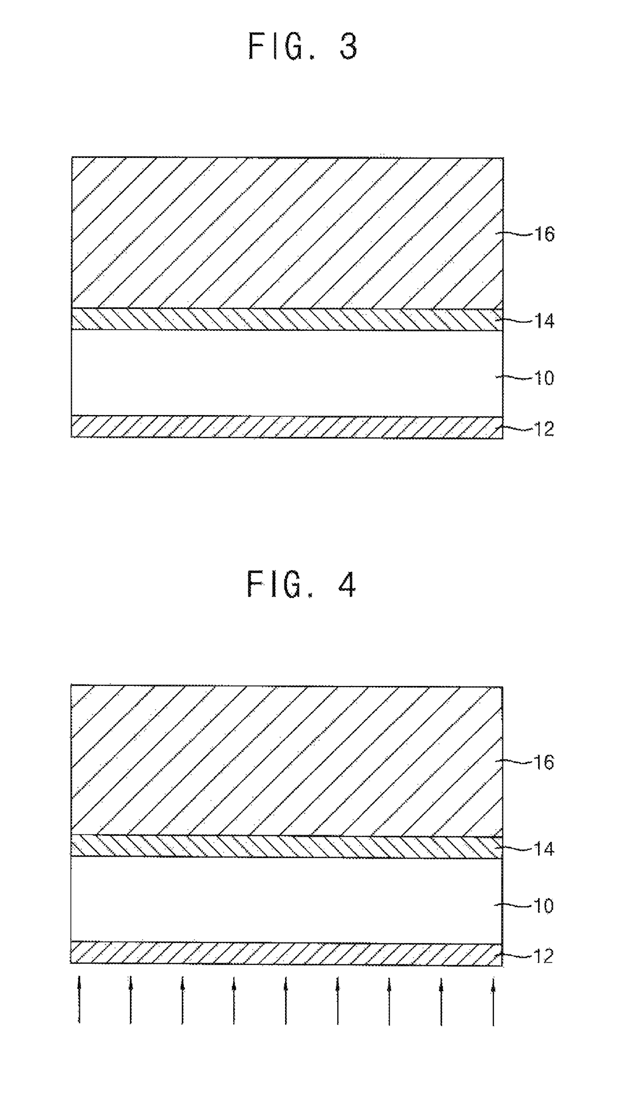
[0016]FIGS. 1 to 6 are cross-sectional views illustrating stages of a method of manufacturing a GaN substrate in accordance with example embodiments.

[0017]Referring to FIG. 1, a silicon substrate 10 may include a second surface 2 on which a GaN substrate 16 (refer to FIG. 3) is formed and a first surface 1 opposite the second surface 2. A capping layer 12 may be formed on the first surface 1 of the silicon substrate 10 to entirely cover the first surface 1 of the silicon substrate 10.

[0018]The silicon substrate 10 may serve as a seed substrate (or a template substrate) for forming the GaN substrate 16. Thus, a diameter of the GaN substrate 16 subsequently formed may be determined by a diameter of the silicon substrate 10.

[0019]The silicon substrate 10 may have a relatively large area. In example embodiments, the silicon substrate 10 may have a thickness of about 100 μm to about 1000 μm, and may have a diameter equal to or more than about 6 inches, e.g., about 6 inches to about 18 in...


PUM

PropertyMeasurementUnit
temperatureaaaaaaaaaa
diameteraaaaaaaaaa
diameteraaaaaaaaaa

Abstract

In a method of manufacturing a GaN substrate, a capping layer may be formed on a first surface of a silicon substrate. A buffer layer may be formed on a second surface of the silicon substrate. The second surface may be opposite the first surface. A GaN substrate may be formed on the buffer layer by performing a hydride vapor phase epitaxy (HVPE) process. The capping layer and the silicon substrate may be removed.

Description

CROSS-REFERENCE TO RELATED APPLICATION[0001]This application claims priority under 35 USC § 119 to Korean Patent Application No. 10-2016-0137596, filed on Oct. 21, 2016 in the Korean Intellectual Property Office (KIPO), the contents of which are herein incorporated by reference in their entirety.BACKGROUND1. Field[0002]Example embodiments relate to a method of manufacturing a gallium nitride (GaN) substrate. More particularly, example embodiments relate to a method of manufacturing a GaN substrate having a large-area.2. Description of the Related Art[0003]A GaN substrate may serve as a substrate of a short-wavelength light-emitting device. In general, a sapphire substrate may be used as a seed substrate for manufacturing the GaN substrate. However, a difference between thermal expansion coefficients of sapphire and GaN may be relatively great, so that the GaN substrate formed on the sapphire substrate may be broken during a temperature lowering process. After the GaN is grown on a s...

Claims


Application Information

Patent Timeline
Patent Type & Authority Patents(United States)
IPC IPC(8): C30B25/02C30B25/18H01L21/02H01L21/78C30B25/10C30B29/40C30B25/16C30B29/06
CPCC30B25/186C30B25/02C30B25/10C30B25/16C30B25/183C30B29/06H01L21/7806H01L21/0254H01L21/0262H01L21/02381H01L21/02458H01L21/02658C30B29/406H01L33/0075H01L33/0093C30B33/12H01L21/02389H01L21/0228H01L21/3065H01L21/31116H01L2924/1033H01L21/02631
Inventor KIM, MI-HYUNKANG, SAM-MOOKKIM, JUN-YOUNTAK, YOUNG-JOPARK, YOUNG-SOO
Owner SAMSUNG ELECTRONICS CO LTD
Learn More