Semiconducting pixel, matrix of such pixels, semiconducting structure for the production of such pixels and their methods of fabrication

a technology of semiconductor pixel and matrix, which is applied in the field of semiconductor pixel, can solve the problems of non-negligible overhead of using three different leds, low luminance of oleds for certain applications, and miniaturization problems, and achieves the effects of less loss, high luminosity, and simple hybridization

Active Publication Date: 2018-10-16
CENT NAT DE LA RECHERCHE SCI
View PDF33 Cites 15 Cited by
  • Summary
  • Abstract
  • Description
  • Claims
  • Application Information

AI Technical Summary

Benefits of technology

[0010]a semi-conducting pixel structure that can be produced from inorganic semi-conductors (therefore, potentially, with high luminosity), in a simple manner, and that can be miniaturized, for example as far as a lateral size of less than or equal to 10 μm;
[0014]In accordance with the invention, these objectives are achieved by virtue of a pixel structure comprising three adjacent sub-pixels, produced by etching on the basis of one and the same structure comprising three (light-emitting) active layers—or only two layers, a third being added subsequently. At least one, and preferably two, of these active layers are pumped electrically, the remaining layer or layers being pumped optically to operate as wavelength converter(s). Such a pixel structure can be produced based on inorganic semi-conductors and therefore exhibit a much higher luminosity than that achievable with OLEDs. With respect to the devices described in document U.S. Pat. No. 8,058,663, the hybridization is much simpler and the losses can be lesser (a single tunnel junction is necessary to make it possible to stop all the etchings on n-doped layers). Moreover, as the structure is etched on both its faces, the etching depth is reduced, thereby allowing a very high degree of miniaturization of the sub-pixels.

Problems solved by technology

However, the use of three different LEDs has a non-negligible cost overhead with respect to a single LED.
Moreover, combining three distinct LEDs for the production of each pixel poses miniaturization problems which become insoluble for applications of screen type with a low pixel size.
However, the luminance of OLEDs is too low for certain applications, such as lighting or “near the eye” projection.
Such a structure is difficult to produce, and above all to hybridize, since it is necessary to independently interconnect several active layers situated at different depths of the stack.
Moreover, the structures described by document U.S. Pat. No. 8,058,663 comprise either a plurality of tunnel junctions intended to be connected in series, or contacts taken on “stairways” etched into semi-conducting layers exhibiting a doping of type p; in both cases, relatively significant electrical resistances are obtained, inducing high losses.
Furthermore, the depths to be etched are relatively significant, thus putting limits on the miniaturization achievable.
Such a thickness is not compatible with a high degree of miniaturization of the pixels (lateral dimensions of the order of some ten μm) because of cross absorption of light between the various pixels.
The structures described in these documents cannot be considered to be monolithic; their fabrication requires gluing steps which are complex to carry out.

Method used


Image

  • Semiconducting pixel, matrix of such pixels, semiconducting structure for the production of such pixels and their methods of fabrication
  • Semiconducting pixel, matrix of such pixels, semiconducting structure for the production of such pixels and their methods of fabrication
  • Semiconducting pixel, matrix of such pixels, semiconducting structure for the production of such pixels and their methods of fabrication

Examples


first embodiment

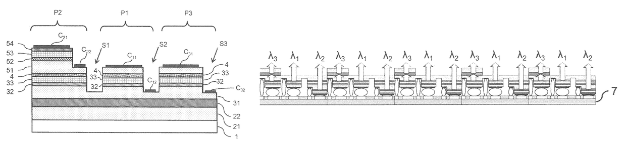
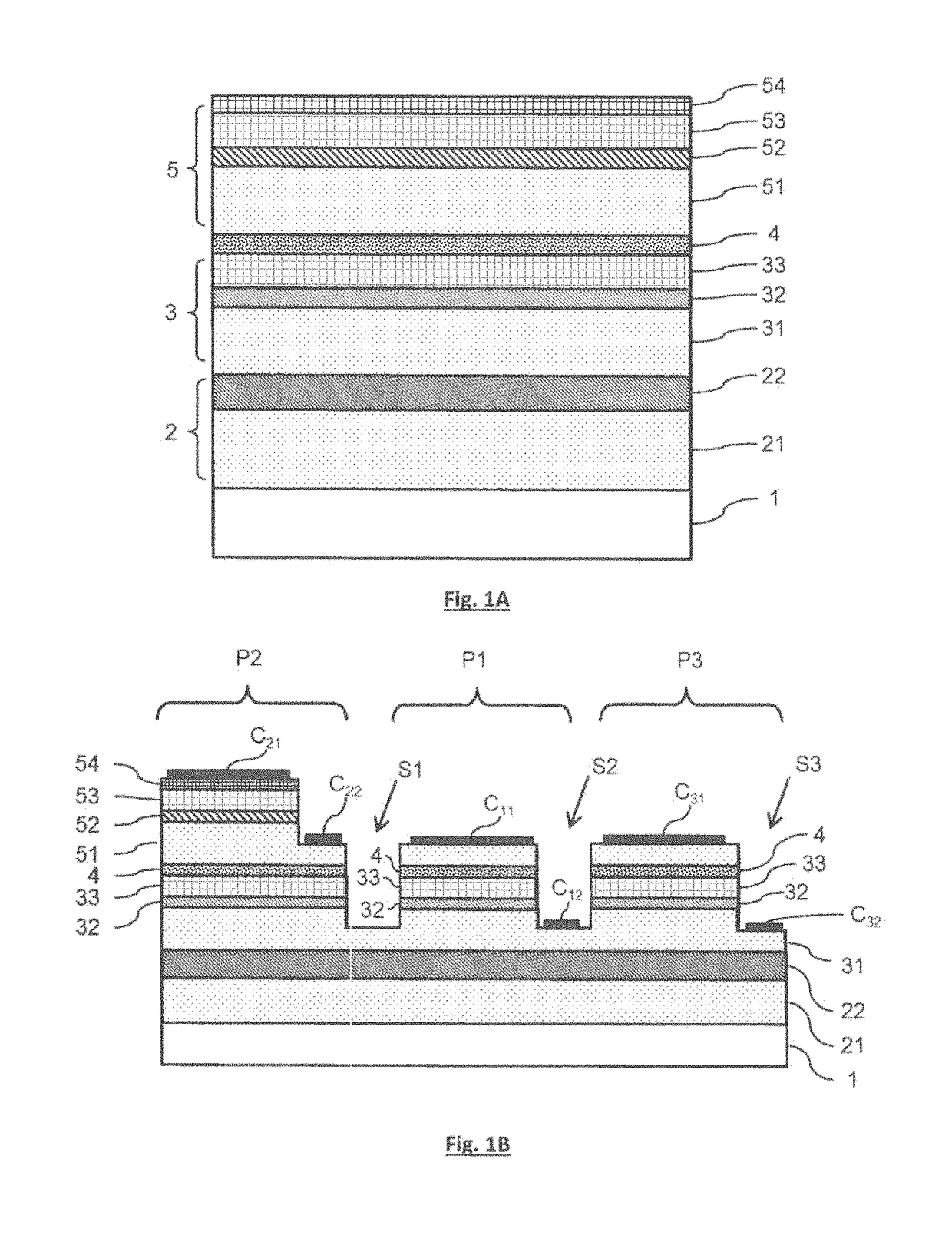
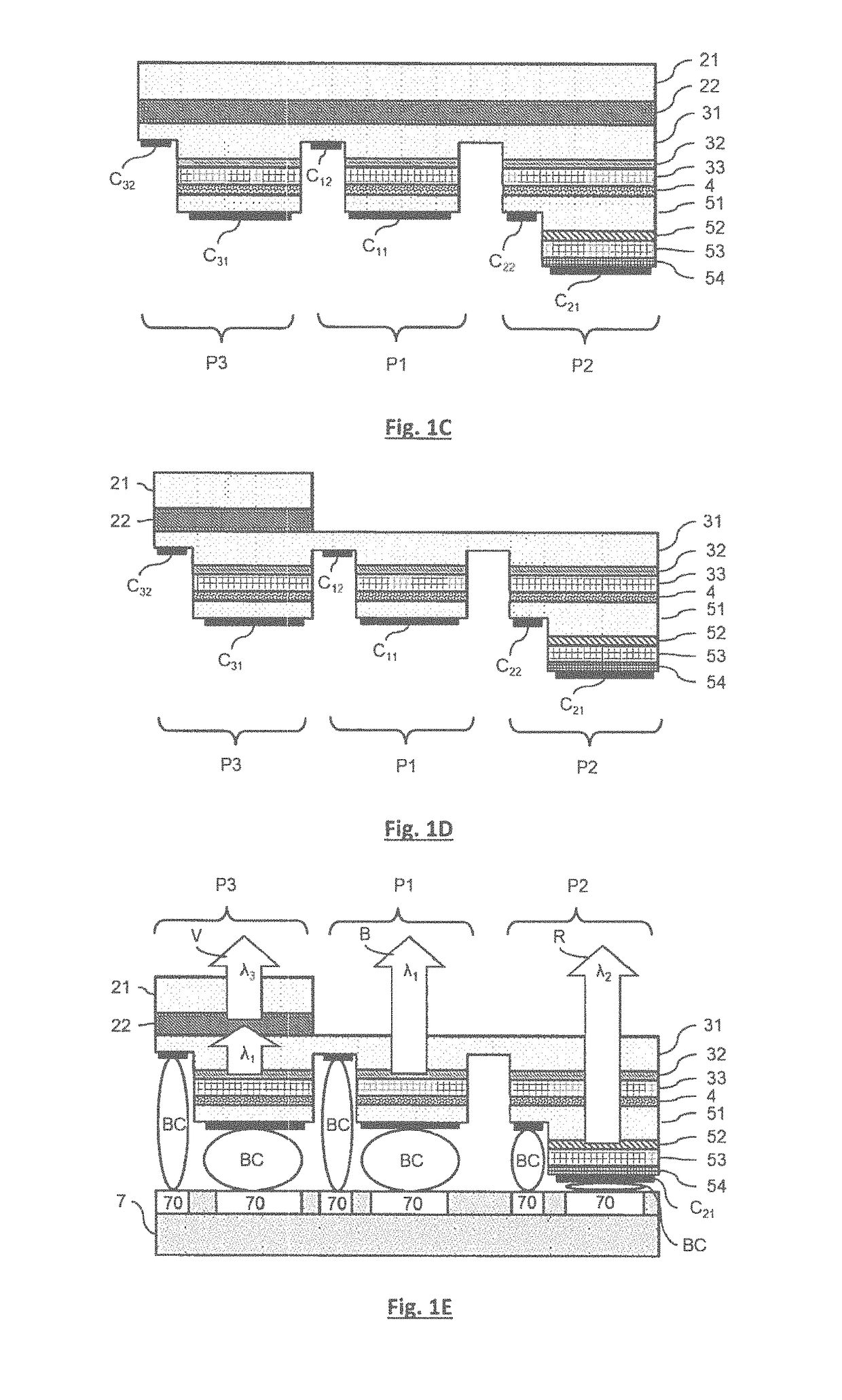
[0054]FIG. 1A shows an epitaxial monolithic structure that can be used as starting point for a method for fabricating a semi-conducting pixel according to the invention. This structure comprises, from the bottom:

[0055]A substrate 1, made for example of sapphire; this substrate will be eliminated in the course of the fabrication method, consequently its nature is of only little importance, provided that it allows the epitaxial growth of the other layers constituting the structure. Thus in place of sapphire it would be possible to use, for example, a substrate made of Si, SiC or ZnO.

[0056]A first subset of semi-conducting layers 2 comprising, in order, a layer 21 of type n doped GaN, for example of thickness equal to 2 μm, having solely an electrical conduction function, and an “active” (that is to say light-emitting) layer 22 comprising a stack of quantum wells (Ga,In)N / (Al,Ga,In)N, also exhibiting a doping of type n or not intentionally doped and able to emit a green luminous radiat...

second embodiment

[0079]FIGS. 2A-2E illustrate the fabrication of a pixel according to the invention, comprising an added wavelength converter, emitting in the red.

[0080]The starting point of such a method (FIG. 2A) is a structure similar to that of FIG. 1A but not comprising the layers 21 and 22; in this structure, the layer 31 is deposited directly on the substrate. Furthermore, the active layer furthest from the substrate (reference 52′) is adapted for emitting a green radiation, instead of a red radiation like the active layer 52 of FIGS. 1A-1E. In FIG. 2A, the reference 3′ identifies a first stack of semi-conducting layers, comprising the layers 31, 32 and 33, and substantially identical to the second stack 3 of FIG. 1A; the reference 5′ identifies a second stack of semi-conducting layers comprising the layers 51, 52′, 53 and 54.

[0081]The first steps of etching (FIG. 2B), inversion and elimination of the substrate (FIG. 2C) are substantially identical to the corresponding steps of the above-desc...


PUM


Abstract

A pixel comprises three adjacent sub-pixels, formed by respective stacks of semi-conducting layers wherein: each sub-pixel comprises a first active layer, adapted for emitting a light at a first wavelength when an electric current passes through it; another sub-pixel comprises a second active layer, adapted for emitting a light at a second wavelength greater than the first wavelength; another sub-pixel comprises a third active layer, adapted for emitting a light at a third wavelength greater than the first wavelength and different from the second wavelength; at least one from among the second and third active layers being adapted for emitting light when it is excited by the light at the first wavelength emitted by the first active layer of the same sub-pixel. Semi-conducting structure and methods for the fabrication of such a pixel are provided.

Description

CROSS-REFERENCE TO RELATED APPLICATIONS[0001]This application is a National Stage of International patent application PCT / EP2015 / 056779, filed on Mar. 27, 2015, which claims priority to foreign French patent application No. FR 1452876, filed on Apr. 1, 2014, the disclosures of which are incorporated by reference in their entirety.FIELD OF THE INVENTION[0002]The invention pertains to a semi-conducting pixel, in particular based on inorganic semi-conductors and more particularly based on (Al,Ga,In)N, as well as to a matrix of such pixels. The invention also pertains to semi-conducting structures serving as a basis for producing such pixels, and to methods for fabricating the latter.[0003]The invention applies in particular to the production of miniaturized color screens and of “near the eye” projectors, as well as to lighting.BACKGROUND[0004]It is known to produce light-emitting devices whose color is obtained and controlled by mixing primary hues. The combination of three light-emitt...

Claims


Application Information

Patent Timeline
Patent Type & Authority Patents(United States)
IPC IPC(8): H01L33/00H01L27/15H01L33/50H01L33/32H01L33/62
CPCH01L27/156H01L33/32H01L33/62H01L33/50H01L2933/0066H01L2933/0041H01L27/153H01L33/08
Inventor DAMILANO, BENJAMINDUBOZ, JEAN-YVES
Owner CENT NAT DE LA RECHERCHE SCI
Why Eureka
Try Eureka