
Semiconductor device

a technology of semiconductors and devices, applied in the direction of semiconductor devices, transistors, electrical equipment, etc., can solve the problems of difficult control of ns, device cannot be made in a normally-off device, etc., to achieve the effect of reducing the increase in on resistance, and improving blocking breakdown voltag

Active Publication Date: 2018-10-23
DENSO CORP
View PDF13 Cites 2 Cited by
  • Summary
  • Abstract
  • Description
  • Claims
  • Application Information

AI Technical Summary

Benefits of technology

The present invention provides a semiconductor device that can suppress degradation of its blocking breakdown voltage and prevent an increase in on resistance. This is achieved by selectively forming a second AlGaN layer in a limited area, while not forming it in areas near the source and drain electrodes. This helps to improve the device's performance and stability. Also, the absence of a 2 DEG under the gate structure makes it a normally-off device. Overall, this patent presents a solution for creating a reliable and efficient semiconductor device.

Problems solved by technology

For this reason, it is difficult to control the Ns.
Therefore, the device cannot be made in a normally-off device.

Method used


Image

  • Semiconductor device
  • Semiconductor device
  • Semiconductor device

Examples


first embodiment

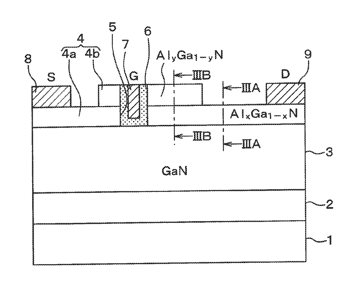
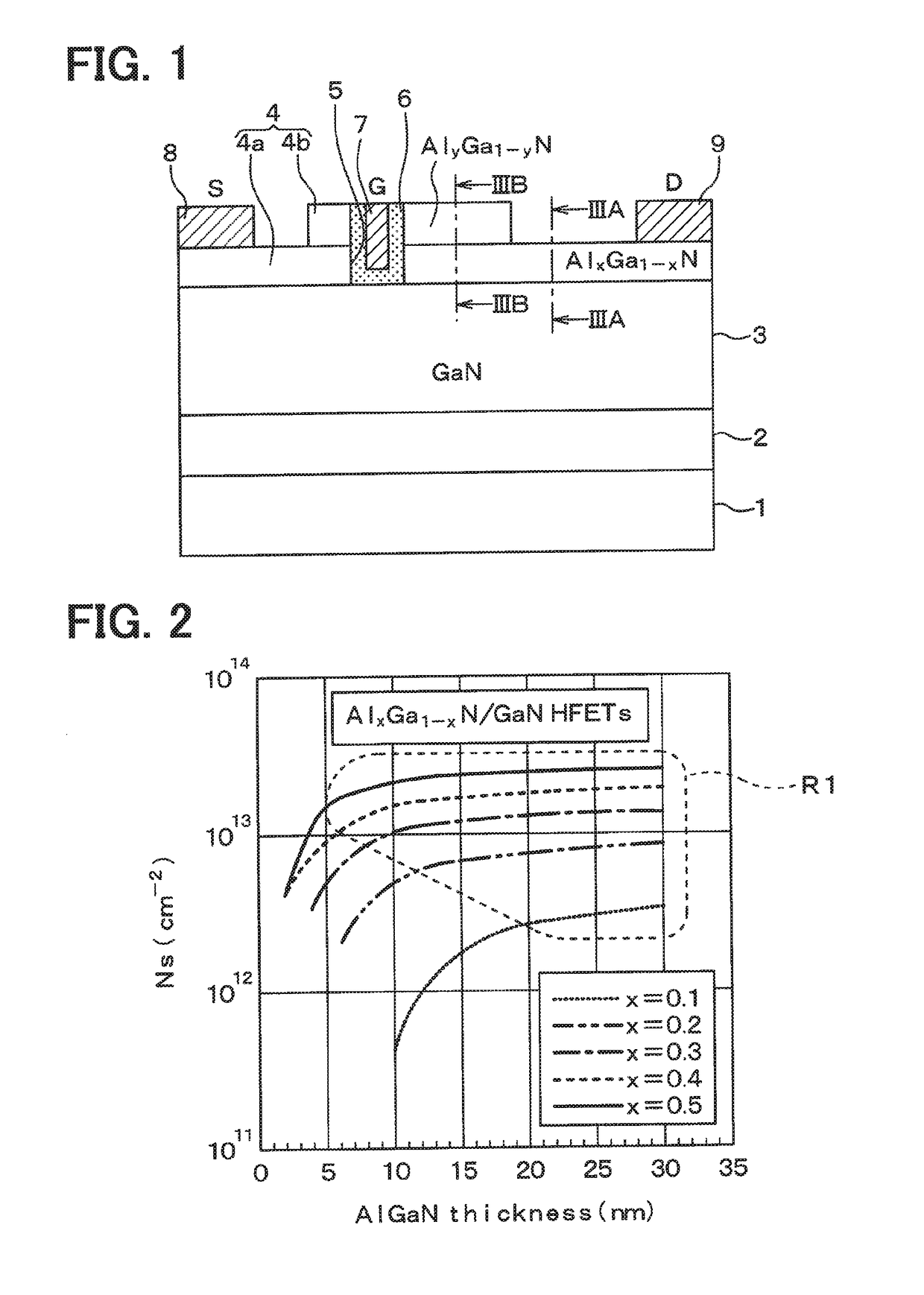
[0032]A first embodiment of the present disclosure will be described with reference to FIG. 1. As shown in FIG. 1, a semiconductor device of the present embodiment is provided with a lateral HEMT as a switching device.

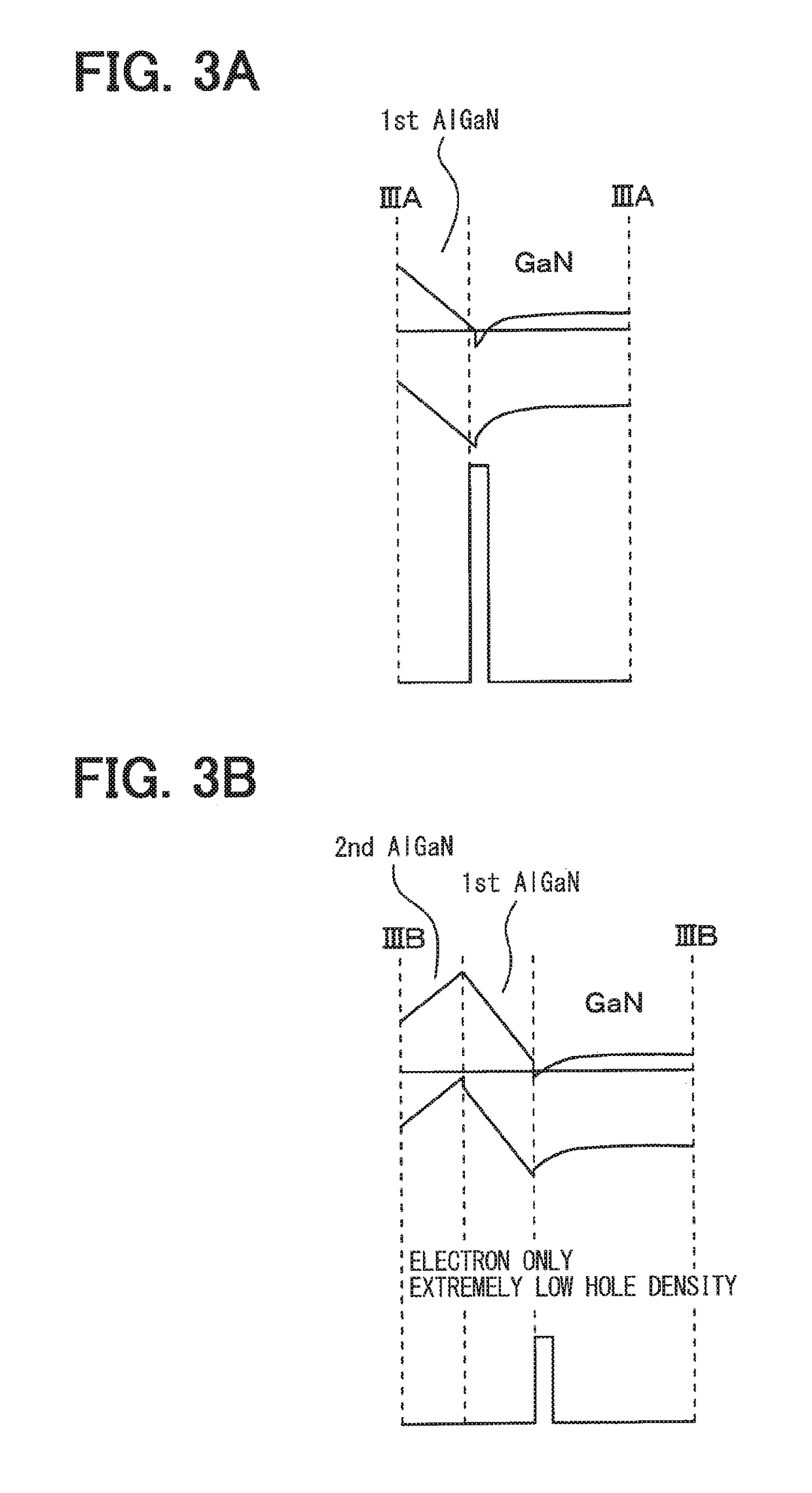
[0033]The lateral HEMT of the present embodiment is provided by employing a structure in which a GaN layer 3 of an i-type, n-type or p-type is laid on a surface of a substrate 1 through a buffer layer 2, as a compound semiconductor substrate. On the surface of the GaN layer 3, an AlGaN layer 4 in which a first AlGaN layer 4a and a second AlGaN layer 4b are layered is formed. The GaN layer 3 and the AlGaN layer 4 form a heterojunction structure. In the lateral HEMT, the GaN layer 3 and the AlGaN layer 4 serve as a channel forming layer. The lateral HEMT operates when the 2 DEG carrier is induced by a piezoelectric effect and a spontaneous polarization effect in the GaN layer 3 adjacent to an AlGaN / GaN interface.

[0034]The substrate 1 is formed of a semi-insulating film o...

second embodiment

[0055]A second embodiment of the present disclosure will be described. In the present embodiment, the structure of the AlGaN layer 4 is modified from that of the first embodiment, and structures other than the AlGaN layer 4 are similar to those of the first embodiment. Therefore, only a part different from the first embodiment will be described.

[0056]As shown in FIG. 6, in the present embodiment, the AlGaN layer 4 has a three-layer structure, which includes a third AlGaN layer 4c between the GaN layer 3 and the first AlGaN layer 4a and the gate structure part. The third AlGaN layer 4c is so thin that the piezoelectric polarization can be remarkably suppressed. The third AlGaN layer 4c is composed of AlzGa1-zN, in which z represents an Al mixed crystal ratio. The Al mixed crystal ratio z of the third AlGaN layer 4c is greater than the Al mixed crystal ratios x, y of the first and second AlGaN layers 4a, 4b.

[0057]In the case where the semiconductor device 4 has the third AlGaN layer ...

third embodiment

[0059]A third embodiment of the present disclosure will be described. In the present embodiment, the structure of the AlGaN layer 4 is modified from that of the first embodiment, and structures other than the AlGaN layer 4 are similar to those of the first embodiment. Therefore, only a part different from the first embodiment will be described.

[0060]In the present embodiment, similarly to the first embodiment, the AlGaN layer 4 has the two-layer structure, as shown in FIG. 7. However, the AlGaN layer 4 includes a fourth AlGaN layer 4d between the first AlGaN layer 4a and the source electrode 8 and the drain electrode 9. The fourth AlGaN layer 4d is spaced from the second AlGaN layer 4b. Therefore, a region where only the first AlGaN layer 4a is formed on the GaN layer 3 remains in between the second AlGaN layer 4b and the fourth AlGaN layer 4d. The fourth AlGaN layer 4d has an Al mixed crystal ratio w, and is composed of AlwGa1-wN. The Al mixed crystal ratio w is greater than the Al...


PUM


Abstract

A semiconductor device includes a lateral switching device having: a substrate; a channel forming layer that has a heterojunction structure made of a GaN layer and an AlGaN layer and is formed with a recessed portion, on the substrate; a gate structure part that includes a gate insulating film and a gate electrode formed in the recessed portion; and a source electrode and a drain electrode on opposite sides of the gate structure part on the channel forming layer. The AlGaN layer includes a first AlGaN layer that has an Al mixed crystal ratio determining a two dimensional electron gas density, and a second AlGaN layer that has an Al mixed crystal ratio smaller than that of the first AlGaN layer to induce negative fixed charge, and is disposed in contact with the gate structure part and spaced from the source electrode and the drain electrode.

Description

CROSS REFERENCE TO RELATED APPLICATIONS[0001]This application is a U.S. national stage of International Patent Application No. PCT / JP2015 / 006089 filed on Dec. 8, 2015 and is based on Japanese Patent Application No. 2014-265668 filed on Dec. 26, 2014, the contents of which are incorporated herein by reference.TECHNICAL FIELD[0002]The present disclosure relates to a semiconductor device having a heterojunction structure made of gallium nitride (hereinafter referred to as GaN), which is a nitride semiconductor, and aluminum gallium nitride (hereinafter referred to as AlGaN).BACKGROUND ART[0003]Patent Literature 1 has proposed a semiconductor device including a HEMT (High electron mobility transistor), which is a field effect transistor, as a lateral switching device having a heterojunction structure with GaN.[0004]The semiconductor device is provided with a lateral HEMT having a heterojunction structure made of GaN and AlGaN. Specifically, the semiconductor device has, on a substrate, ...

Claims


Application Information

Patent Timeline
Patent Type & Authority Patents(United States)
IPC IPC(8): H01L29/66H01L29/778H01L29/786H01L29/06H01L29/40H01L29/51H01L29/423H01L29/20
CPCH01L29/778H01L29/06H01L29/0657H01L29/7786H01L29/786H01L29/66462H01L29/2003H01L29/402H01L29/4236H01L29/518
Inventor OYAMA, KAZUHIROHIGUCHI, YASUSHIOOSAWA, SEIGOMATSUI, MASAKIEUM, YOUNGSHIN
Owner DENSO CORP
Learn More