Printed circuit board and optical module

a printed circuit board and optical module technology, applied in the direction of waveguides, high-frequency circuit adaptations, sustainable manufacturing/processing, etc., can solve the problems of difficult reduction of differential impedance, difficulty in reducing center-to-center distance of differential vias, etc., to reduce differential impedance, reduce differential impedance, reduce the effect of self-inductan

Active Publication Date: 2018-10-30
LUMENTUM JAPAN INC
View PDF6 Cites 13 Cited by
  • Summary
  • Abstract
  • Description
  • Claims
  • Application Information

AI Technical Summary

Benefits of technology

[0010]The present invention has been made in view of the problem described above, and has an object to provide a printed circuit board configured to achieve reduction in impedance of a differential transmission line extending in the printed circuit board in a stacking direction, and an optical module.

Problems solved by technology

However, the above-mentioned prior arts have no particular description about differential transmission lines having a differential impedance that is lower than 100Ω, which are sometimes desired.
However, when the via diameter of the differential via is increased in order to reduce the self inductance, it is difficult to reduce the center-to-center distance of the pair of differential vias due to increase in via diameter.
That is, the reduction in self inductance and the increase in mutual inductance cannot be achieved at the same time, which leads to a difficulty in reduction in differential impedance.

Method used


Image

  • Printed circuit board and optical module
  • Printed circuit board and optical module
  • Printed circuit board and optical module

Examples


first embodiment

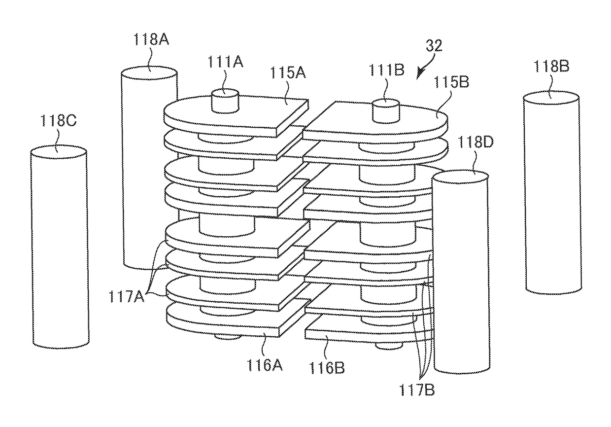
[0072]FIG. 1 is a schematic view for illustrating the configurations of a transmission device 1 and an optical module 2 according to a first embodiment of the present invention. The transmission device 1 includes a printed circuit board 11. Further, the optical module 2 includes a printed circuit board 21. One or both of those printed circuit boards 11 and 21 correspond to a printed circuit board according to the first embodiment.

[0073]The transmission device 1 further includes ICs 12. The transmission device 1 is, for example, a router or a switch having large capacity. The transmission device 1 has, for example, the function of a switch, and is installed in a base station or the like. The transmission device 1 obtains reception data (reception electric signal) by the optical module 2, and determines the destination and type of data to be transmitted, with the use of the IC 12 and the like. Then, the transmission device 1 generates transmission data (transmission electric signal), ...

second embodiment

[0136]FIG. 6A and FIG. 6B are schematic plan views for illustrating part of the structure of a printed circuit board 42 according to a second embodiment of the present invention. The printed circuit board 42 according to the second embodiment has the same structure as that of the printed circuit board 31 according to the first embodiment except that the shapes and dimensions of a differential transmission line included in the printed circuit board 42 according to the second embodiment differ from those of the first embodiment. The optical module 2 according to the second embodiment includes the printed circuit board 42 as the printed circuit board 21. A desired differential impedance can be obtained by increasing or reducing the gap Gap illustrated in FIG. 6B. Here, it is described that connection having satisfactory characteristics is achieved with at least a differential transmission line having a differential impedance value within a range of from 50Ω to 60Ω. The differential imp...

third embodiment

[0142]FIG. 8A and FIG. 8B are schematic plan views for illustrating part of the structure of a printed circuit board 43 according to a third embodiment of the present invention. FIG. 8C is a schematic cross-sectional view for illustrating part of the printed circuit board 43 according to the third embodiment. FIG. 8C is an illustration of a cross section taken along the line VIIIC-VIIIC of FIG. 8A. The printed circuit board 43 according to the third embodiment has the same structure as that of the printed circuit board 31 according to the first embodiment except for the following points. The shape of each of the plurality of conductor plate pairs 102 of a differential transmission line included in the printed circuit board 43 according to the third embodiment differs from that of the first embodiment. Correspondingly, the shapes of the first strip conductor pair 104, the second strip conductor pair 105, the first through hole 119, and the second through hole 129 differ from those of...


PUM


Abstract

Provided are a printed circuit board configured to achieve reduction in impedance of a differential transmission line extending in a stacking direction, and an optical module. The printed circuit board includes a stacking-direction differential transmission line extending in the stacking direction, including: a differential signal via pair including a first signal via and a second signal via; and a plurality of conductor plate pairs each including a first conductor plate expanding outward from the first signal via, and a second conductor plate expanding outward from the second signal via. With respect to a perpendicular bisector of a center-of-gravity line segment connecting centers of gravity of the first and second signal vias, in each of the plurality of conductor plate pairs, centers of gravity of contours of the first and second conductor plates are located on inner sides of the centers of gravity.

Description

CROSS-REFERENCE TO RELATED APPLICATION[0001]The present application claims priority from Japanese application JP 2016-096791, filed on May 13, 2016, the content of which is hereby incorporated by reference into this application.BACKGROUND OF THE INVENTION1. Field of the Invention[0002]The present invention relates to a printed circuit board and an optical module, and more particularly, to suppression of the differential impedance of a differential transmission line arranged on a printed circuit board.2. Description of the Related Art[0003]A transmission line is formed on a printed circuit board, and electric signals (e.g., serial data signals) are transmitted with the use of the transmission line. Examples of the transmission line include a micro strip line. When a differential transmission line is achieved with a micro strip line, the micro strip line includes a ground conductor layer and a pair of strip conductor layers arranged via a dielectric layer. The micro strip line can be ...

Claims


Application Information

Patent Timeline
Patent Type & Authority Patents(United States)
IPC IPC(8): H01S5/022H01P5/04H05K1/11H05K1/18H01P3/02H01P3/08H01S5/042H05K1/02
CPCH01S5/02248H01P3/026H01P3/081H01P5/04H05K1/0245H05K1/115H05K1/181H01S5/0427H05K2201/10121H01L33/62H05K1/0251H05K2201/0776H05K1/0298H05K1/141Y02P70/50H01S5/02325
Inventor KAGAYA, OSAMUTAKAHASHI, KOYUISHII, HIROYOSHI
Owner LUMENTUM JAPAN INC
Why Eureka
Try Eureka