Chip package structure with conductive pillar and a manufacturing method thereof

Active Publication Date: 2018-12-18
POWERTECH TECHNOLOGY
View PDF11 Cites 25 Cited by
  • Summary
  • Abstract
  • Description
  • Claims
  • Application Information

AI Technical Summary

Benefits of technology

[0009]In light of the foregoing, in the present invention, at least one semiconductor component is disposed on the first carrier, and the conductive pillars are formed on the semiconductor component. Then, the encapsulant is formed to encapsulate the semiconductor component and expose the top surface of the conductive pillars, and the redistribution layer is formed on the encapsulant to electrically connect the semiconductor component. Then, multiple semiconductor component are sequentially stacked on the redistribution layer, and the steps of forming conductive pillars/through pillars, encapsulant and redistribution layer may be repeated to form the stacked type chip package structure. Accordingly, the thic

Problems solved by technology

As a result, the device including a semico

Method used


Image

  • Chip package structure with conductive pillar and a manufacturing method thereof
  • Chip package structure with conductive pillar and a manufacturing method thereof
  • Chip package structure with conductive pillar and a manufacturing method thereof

Examples


Example

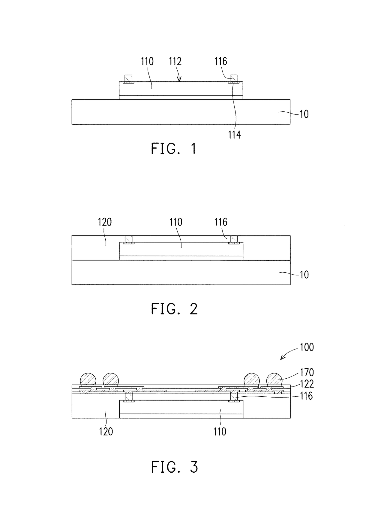
[0018]Reference will now be made in detail to the present preferred embodiments of the invention, examples of which are illustrated in the accompanying drawings. Wherever possible, the same reference numbers are used in the drawings and the description to refer to the same or like parts.

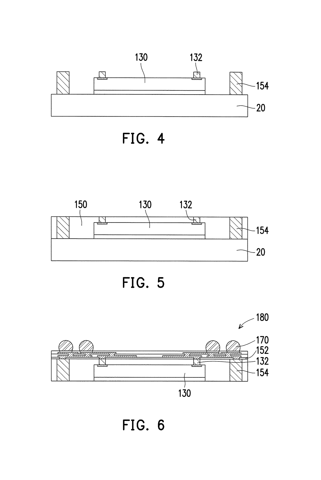
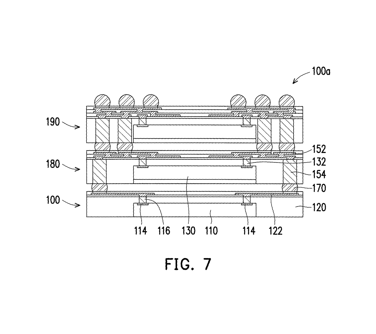
[0019]FIG. 1 to FIG. 7 illustrate cross-sectional views of a manufacturing process of a chip package structure according to an embodiment of the invention. In the present embodiment, a manufacturing process of a chip package structure may include the following steps. Referring to FIG. 1, a first semiconductor component 110 is disposed on a first carrier 10 as shown in FIG. 1. The first semiconductor component 110 may be a chip. The first semiconductor component 110 may include a first active surface 112 and a plurality of first pads 114 disposed on the first active surface 112. Then, a plurality of first conductive pillars 116 are formed on the first pads 114. Each of the first conductive pillars 116...


PUM


Abstract

A chip package structure includes a semiconductor component, a plurality of conductive pillars, an encapsulant and a redistribution layer. The semiconductor component includes a plurality of pads. The conductive pillars are disposed on the pads, wherein each of the conductive pillars is a solid cylinder including a top surface and a bottom surface, and a diameter of the top surface is substantially the same as a diameter of the bottom surface. The encapsulant encapsulates the semiconductor component and the conductive pillars, wherein the encapsulant exposes the top surface of each of the conductive pillars. The redistribution layer is disposed on the encapsulant and electrically connected to the conductive pillars.

Description

CROSS REFERENCE TO RELATED APPLICATION[0001]This application claims the priority benefit of U.S. provisional application Ser. No. 62 / 385,257, filed on Sep. 9, 2016. The entirety of the above-mentioned patent application is hereby incorporated by reference herein and made a part of specification.BACKGROUND OF THE INVENTIONField of the Invention[0002]The present invention generally relates to chip package structure and a manufacturing method thereof. More particularly, the present invention relates to a stacked type chip package structure and a manufacturing method thereof.Description of Related Art[0003]Recently, attention has paid to a semiconductor device called a “substrate with a built-in chip” in which a chip and the like are buried in a substrate made of resin and the like and a semiconductor device in which an insulating layer and a wiring layer are formed on the chip. In semiconductor devices such as a substrate with a built-in chip, it is necessary to bury a chip in the insu...

Claims


Application Information

Patent Timeline
IPC IPC(8): H01L23/522H01L23/00H01L23/31H01L25/04H01L21/56H01L25/00
CPCH01L23/5226H01L21/56H01L23/3107H01L24/11H01L24/27H01L24/32H01L25/04H01L25/50H01L24/14H01L2224/32145H01L23/3121H01L23/49838H01L23/528H01L25/071H01L2225/06527H01L2224/24147H01L23/49816H01L23/5389H01L25/03H01L25/0657H01L25/105H01L2224/04105H01L2224/12105H01L2224/16227H01L2224/73267H01L2225/1035H01L2225/1058H01L2924/1532H01L2924/18162H01L2225/06524H01L2225/06568H01L23/3128H01L21/568H01L21/6835H01L2221/68359H01L24/19H01L2224/92244H01L2224/83005H01L2224/32225H01L24/20H01L24/73H01L24/92
Inventor HSU, HUNG-HSINLIN, NAN-CHUN
Owner POWERTECH TECHNOLOGY
Why Eureka
Try Eureka