

Accurate, low-power power detector circuits and related methods using programmable reference circuitry
- Summary
- Abstract
- Description
- Claims
- Application Information
AI Technical Summary
Benefits of technology
Problems solved by technology
Method used
Image

Examples
first embodiment
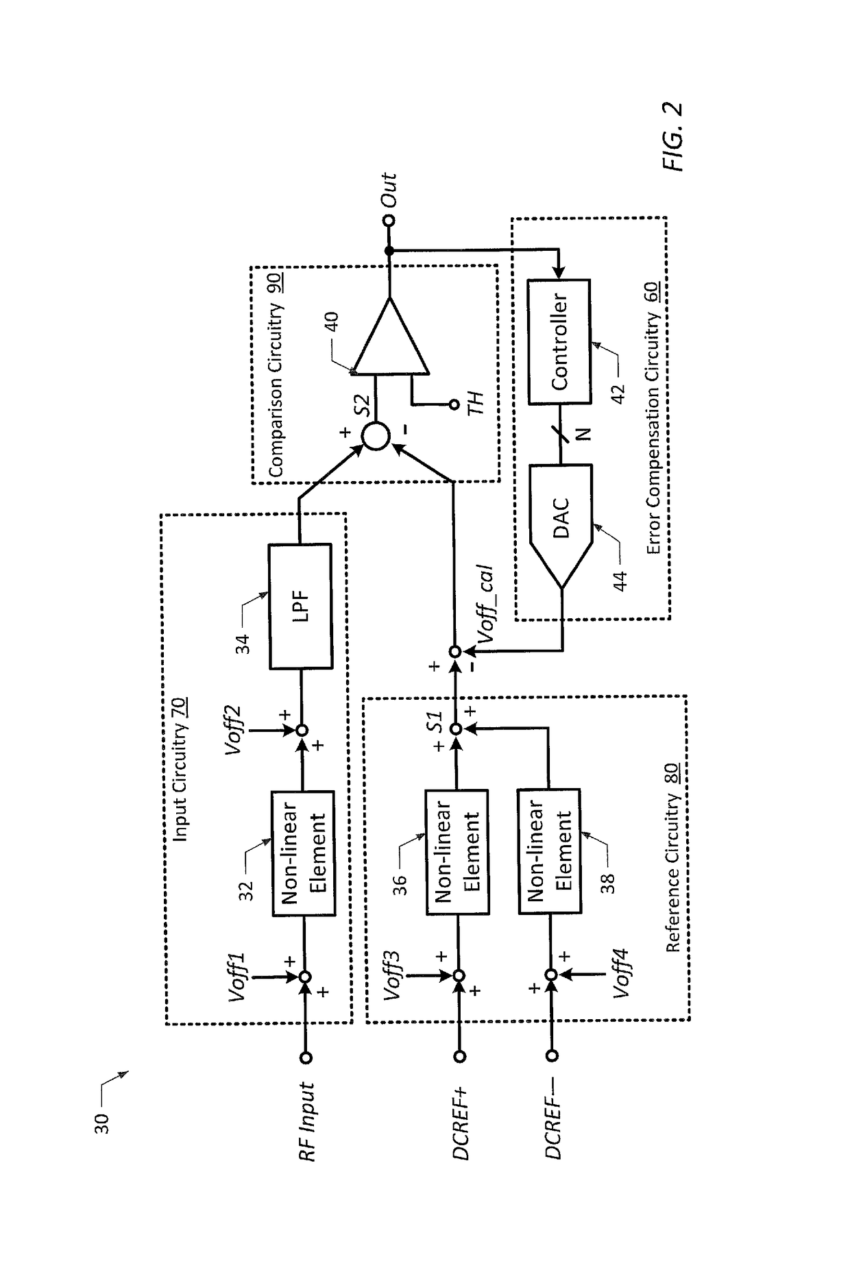
[0047]FIG. 2 illustrates power detector circuit 30, which includes error compensation circuitry that is configured to select an adjustable DC calibration signal (Voff_cal) based on the power measurement signal (Out), and is coupled to supply the selected DC calibration signal to the input circuitry 70, or to the reference circuitry 80, to compensate for the DC offsets (Voff1, Voff2, Voff3, and Voff4) generated within the power detector circuit. In the illustrated embodiment, the error compensation circuitry includes controller 42 and digital-to-analog converter (DAC) 44. Controller 42 is coupled to receive the power measurement signal (Out) from comparator 40, and is configured to select an N-bit programmable digital input value that ensures the selected DC calibration signal (Voff_cal) will compensate for the DC offsets (Voff1, Voff2, Voff3, and Voff4). According to one embodiment, controller 42 is a digital control block that receives a one-bit digital input signal (Out) and gener...
second embodiment
[0058]FIG. 4 illustrates power detector circuit 30, which includes error compensation circuitry 60 that is configured to select an adjustable gain based on the power measurement signal (Out), and is coupled to supply the selected gain to the input circuitry 70, or to the reference circuitry 80, to compensate the undesired DC offsets (Voff1, Voff2, Voff3, and Voff4) generated within the power detector circuit. In the illustrated embodiment, the error compensation circuitry 60 includes variable gain element 48 in the RF input signal path, and controller 46 which is coupled to control the gain of the variable gain element with an M-bit programmable digital value (a programmable gain value). Controller 46 is coupled to receive the power measurement signal (Out) from comparator 40, and is configured to select the M-bit programmable digital input value that ensures the selected gain will compensate for the undesired DC offsets (Voff1, Voff2, Voff3, and Voff4). According to one embodiment,...
third embodiment
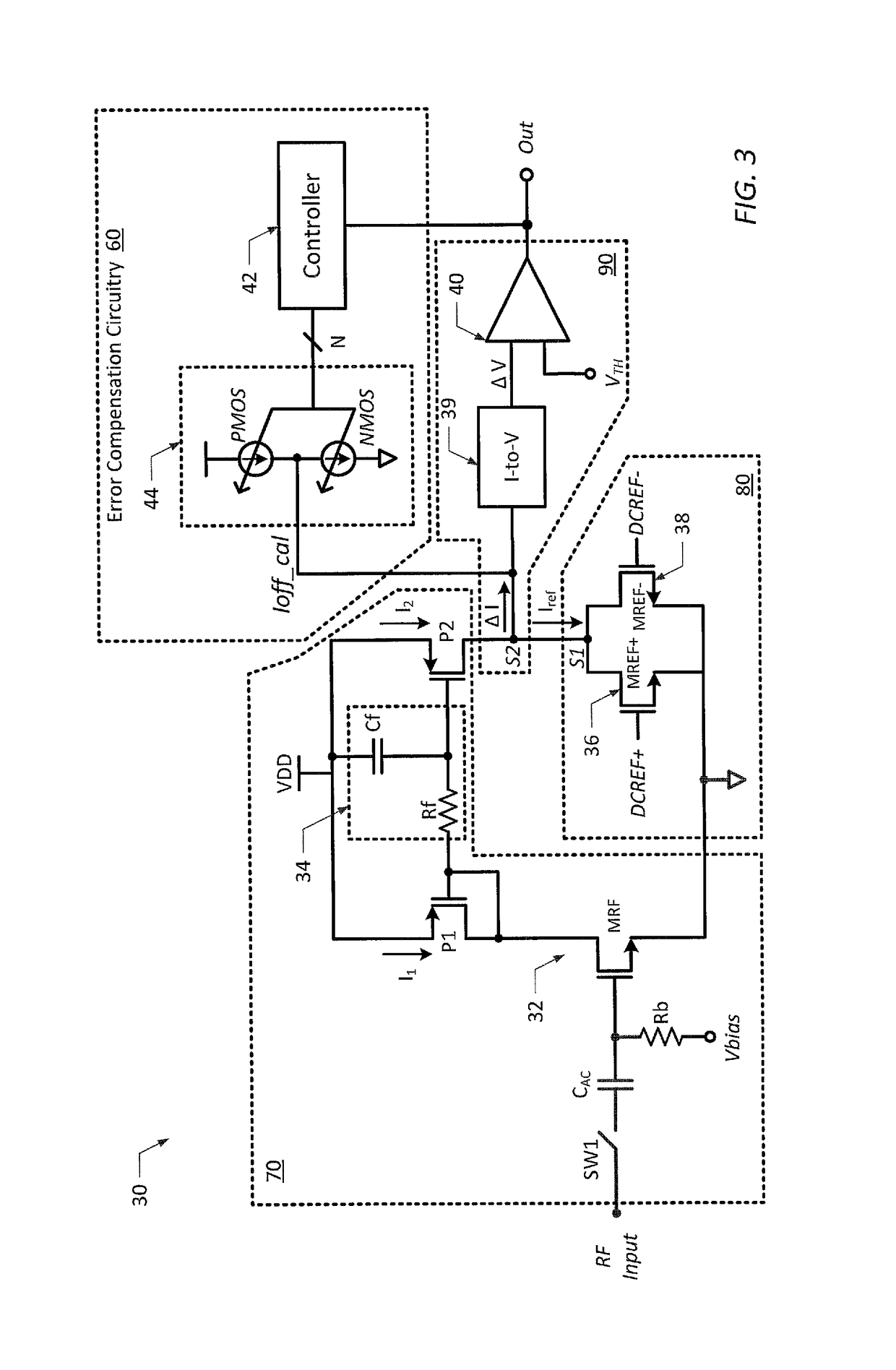
[0068]FIG. 8 illustrates power detector circuit 30, which includes error compensation circuitry 60 that is configured to select an adjustable digital input value, which when supplied to the reference circuitry 80, compensate for the undesired DC offsets (Voff1, Voff2, Voff3, and Voff4) generated within the power detector circuit.
[0069]Like the previously disclosed embodiments, the power detector circuit 30 shown in FIG. 8 includes input circuitry 70, reference circuitry 80, comparison circuitry 90 and error compensation circuitry. As in the previous embodiments, the input circuitry 70 includes a first non-linear element 32 coupled to receive the RF input signal, and a low pass filter 34 coupled to the first non-linear element for generating a magnitude signal, which includes a DC component proportional to the power of the RF input signal, and includes undesired DC offsets (Voff1, Voff2). Likewise, the reference circuitry 80 includes a pair of non-linear elements 36 and 38, which are...
PUM
 Abstract
Description
Claims
Application Information