Method for fabricating buried word line of a dynamic random access memory

a dynamic random access memory and buried word technology, applied in semiconductor devices, semiconductor/solid-state device details, electrical devices, etc., can solve the problems that current dram units with buried gate structures still pose numerous problems, and achieve the effect of improving adhesion and lowering the resistance of the devi

Active Publication Date: 2019-02-19
UNITED MICROELECTRONICS CORP +1
View PDF7 Cites 0 Cited by
  • Summary
  • Abstract
  • Description
  • Claims
  • Application Information

AI Technical Summary

Benefits of technology

[0005]According to an embodiment of the present invention, the formation of the barrier layer preferably includes reacting a first reagent containing titanium with a second reagent containing nitrogen to form a barrier layer made of titanium nitride (TiN) and a byproduct containing Ti(NH2)xCly. Next, a soaking process is conducted thereafter to remove the byproduct for improving adhesion between the barrier layer and the conductive layer and at the same time lowering resistance of the device.

Problems solved by technology

Nevertheless, current DRAM units with buried gate structures still pose numerous problems due to limited fabrication capability.

Method used


Image

  • Method for fabricating buried word line of a dynamic random access memory
  • Method for fabricating buried word line of a dynamic random access memory
  • Method for fabricating buried word line of a dynamic random access memory

Examples


Embodiment Construction

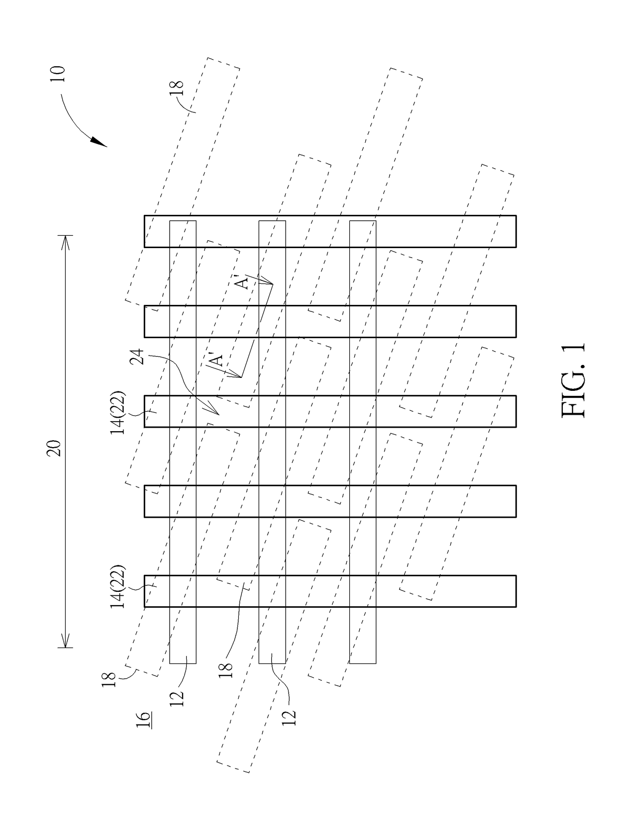
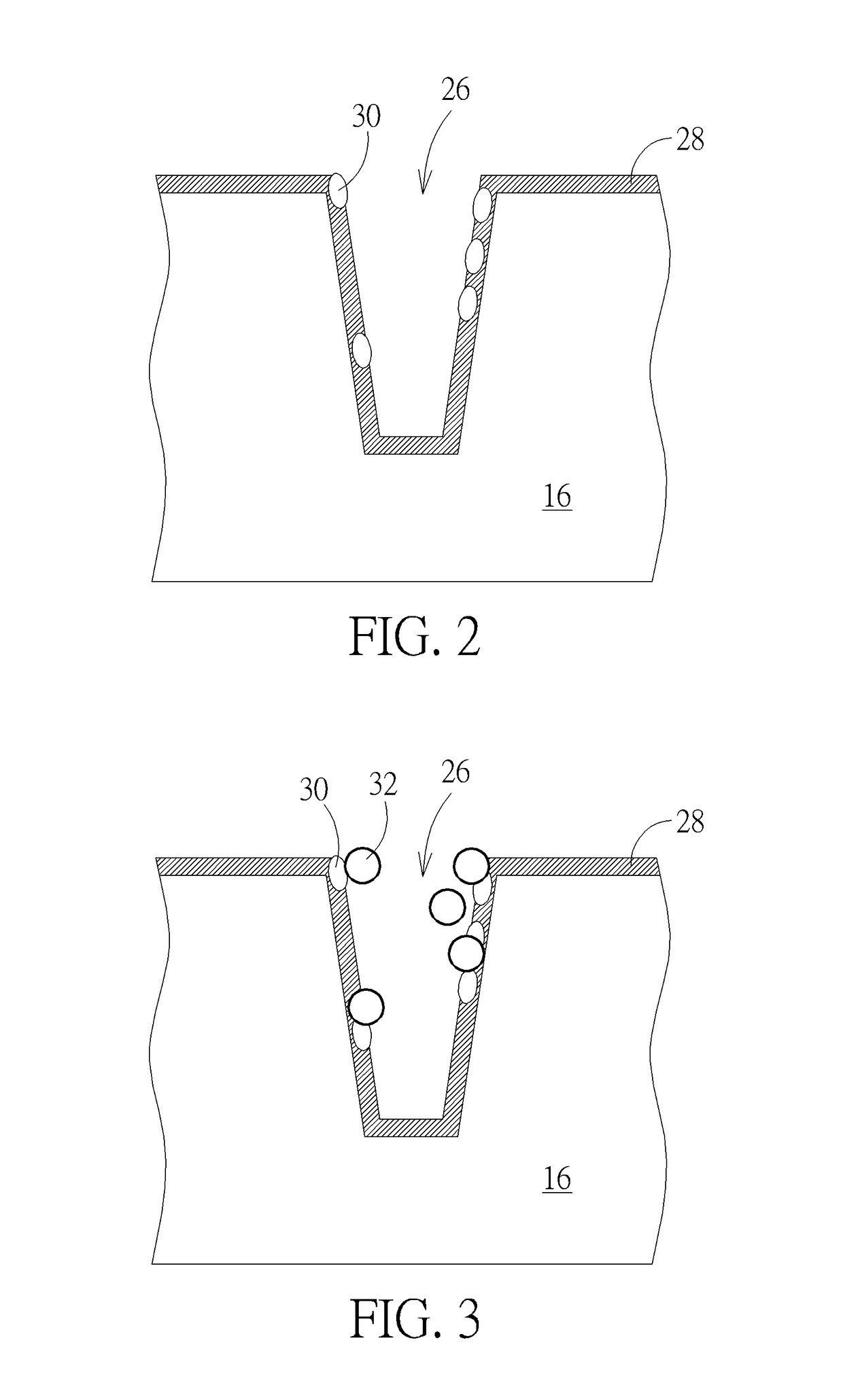
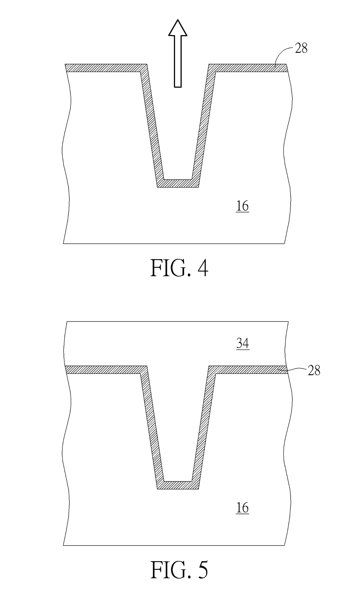
[0008]Referring to FIGS. 1-6, FIGS. 1-6 illustrate a method for fabricating a DRAM device according to an embodiment of the present invention, in which FIG. 1 illustrates a top-view diagram of a DRAM device and FIGS. 2-6 illustrate cross-sectional views of a method for fabricating a buried word line (BWL) of the DRAM device along the sectional line AA′ of FIG. 1. Preferably, the present embodiment pertains to fabricate a memory device, and more particularly a DRAM device 10, in which the DRAM device 10 includes at least a transistor device (not shown) and at least a capacitor structure (not shown) that will be serving as a smallest constituent unit within the DRAM array and also used to receive electrical signals from bit lines 12 and word lines 14.

[0009]As shown in FIG. 1, the DRAM device 10 includes a substrate 16 such as a semiconductor substrate or wafer made of silicon, a shallow trench isolation (STI) 24 formed in the substrate 16, and a plurality of active areas (AA) 18 defin...


PUM


Abstract

A method for fabricating a buried word line (BWL) of a dynamic random access memory (DRAM) includes the steps of: forming a trench in a substrate; forming a barrier layer in the trench; performing a soaking process to reduce chlorine concentration in the barrier layer; and forming a conductive layer to fill the trench.

Description

BACKGROUND OF THE INVENTION1. Field of the Invention[0001]The invention relates to a method for fabricating semiconductor device, and more particularly to a method for fabricating buried word line (BWL) of a dynamic random access memory (DRAM) device.2. Description of the Prior Art[0002]As electronic products develop toward the direction of miniaturization, the design of dynamic random access memory (DRAM) units also moves toward the direction of higher integration and higher density. Since the nature of a DRAM unit with buried gate structures has the advantage of possessing longer carrier channel length within a semiconductor substrate thereby reducing capacitor leakage, it has been gradually used to replace conventional DRAM unit with planar gate structures.[0003]Typically, a DRAM unit with buried gate structure includes a transistor device and a charge storage element to receive electrical signals from bit lines and word lines. Nevertheless, current DRAM units with buried gate st...

Claims


Application Information

Patent Timeline
Patent Type & Authority Patents(United States)
IPC IPC(8): H01L29/423H01L21/768H01L21/3205H01L29/49H01L29/778H01L29/45H01L23/535H01L21/02H01L23/532H01L27/108H01L21/4763
CPCH01L27/10891H01L21/76852H01L23/53266H01L21/02068H01L23/535H01L21/76895H01L21/321H01L21/76861H01L21/76843H10B12/488
Inventor CHANG, KAI-JIUNCHEN, YI-WEICHENG, TSUN-MINWU, CHIA-CHENCHEN, PIN-HONGTSAI, CHIH-CHIEHCHEN, TZU-CHIEHHUANG, YI-AN
Owner UNITED MICROELECTRONICS CORP
Why Eureka
Try Eureka