Bias control for stacked transistor configuration

a transistor and configuration technology, applied in the field of amplifiers, can solve the problems of undesirable use of linear modulation schemes for nonlinear power amplifiers, and achieve the effects of increasing the output power linearity of amplifiers, and decreasing the voltage level of varying supply voltages

Active Publication Date: 2019-03-26
PSEMI CORP
View PDF32 Cites 9 Cited by
  • Summary
  • Abstract
  • Description
  • Claims
  • Application Information

AI Technical Summary

Benefits of technology

[0009]According to a fifth aspect of the present disclosure, a method of increasing output power linearity of an amplifier is presented, the method comprising: i) providing an amplifier comprising stacked transistors in a cascode configuration; ii) applying a high voltage level of a varying supply voltage to a drain of an output transistor of the stacked transistors; iii) based on the applying, providing fixed bias voltages to gate terminals of the stacked transistors; iv) based on the providing, distributing the high voltage level across the stacked transistors; v) based on the distributing, controlling the stacked transistors to operate in their respective saturation regions of operation; vi) decreasing a voltage level of the varying supply voltage; vii) based on the decreasing, keep providing the fixed bias voltages; viii) based on the decreasing and the keep providing, maintaining operation of the stacked transistors within their respective regions of operation; ix) further decreasing the voltage level of the varying supply voltage; x) based on the further decreasing, keep providing the fixed bias voltages; xi) based on the further decreasing and the keep providing, maintaining operation of an input transistor of the stacked transistors within its saturation region of operation, while allowing other transistors of the stacked transistors to transition to their respective triode regions of operation; xii) based on the maintaining operation of the input transistor within its saturation region of operation, increasing an output power linearity of the amplifier, wherein the output power linearity is based on a linear relationship between an output power of a signal amplified by the amplifier and the voltage level of the varying power supply.

Problems solved by technology

Although nonlinear amplifiers can exhibit higher efficiency than linear amplifiers, until recently nonlinear power amplifiers were undesirable for use with RF signals produced by linear modulation schemes.

Method used


Image

  • Bias control for stacked transistor configuration
  • Bias control for stacked transistor configuration
  • Bias control for stacked transistor configuration

Examples


Embodiment Construction

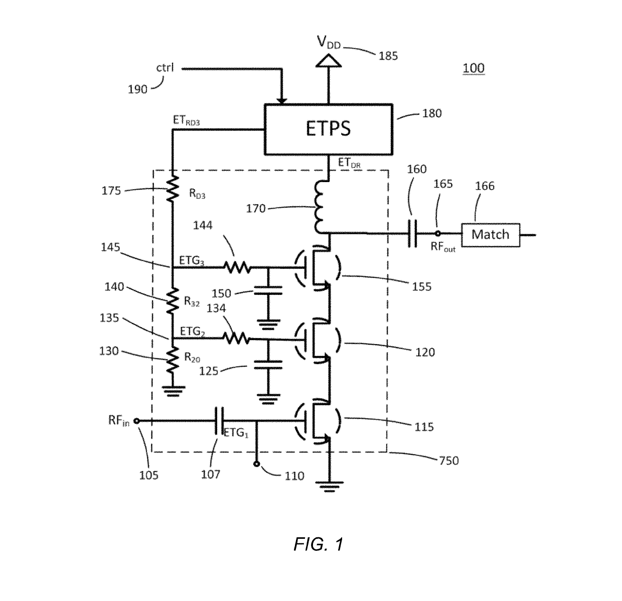
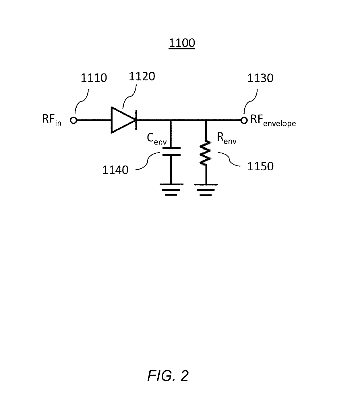
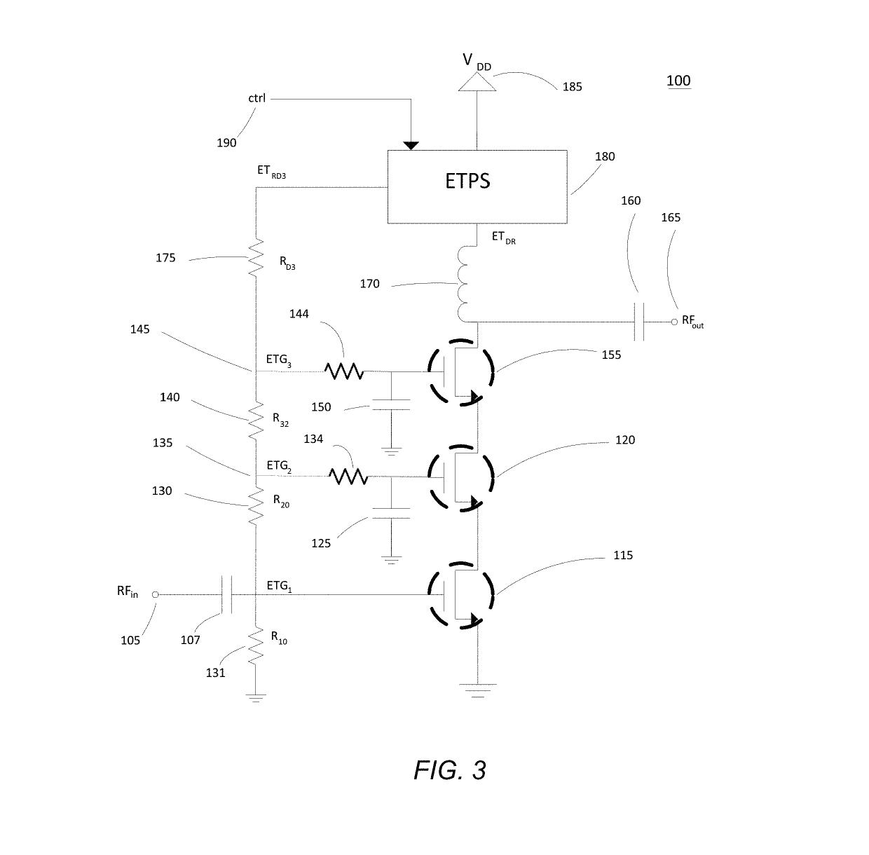
[0106]The present disclosure describes methods and arrangements for amplifier dynamic bias adjustment for envelope tracking and other applications where the supply voltage to the amplifier varies. Furthermore, configuration methods and arrangements using such amplifiers as well as related system integration and controls are presented. Such amplifiers may be used within mobile handsets for current communication systems (e.g. WCMDA, LTE, GSM, etc.) wherein amplification of signals with frequency content of above 100 MHz and at power levels of above 50 mW is required. Such amplifiers may also be used to transmit power at frequencies and to loads as dictated by downstream splitters, cables, or feed network(s) used in delivering cable television service to a consumer, a next amplifier in an RF chain at a cellular base station; or a beam forming network in a phased array radar system, and other. The skilled person may find other suitable implementations for the present disclosure, targete...


PUM


Abstract

Various methods and circuital arrangements for biasing one or more gates of stacked transistors of an amplifier are presented, where the amplifier can have a varying supply voltage that varies according to a control voltage. The control voltage can be related to a desired output power of the amplifier and / or to an envelope signal of an input signal to the amplifier. Particular biasing for selectively controlling the stacked transistors to operate in either a saturation region or a triode region is also presented. Benefits of such controlling, including increased linear response of an output power of the amplifier, are also discussed.

Description

CROSS REFERENCE TO RELATED APPLICATIONS—CLAIM OF PRIORITY[0001]The present application is a continuation in part of U.S. application Ser. No. 14 / 626,833 filed on Feb. 19, 2015 which in turn is a continuation in part of U.S. patent application Ser. No. 13 / 829,946 filed on Mar. 14, 2013 which in turn claims priority to: U.S. provisional application No. 61 / 747,009 filed on Dec. 28, 2012, U.S. provisional application No. 61 / 747,016 filed on Dec. 28, 2012, U.S. provisional application No. 61 / 747,025 filed on Dec. 28, 2012, and U.S. provisional application No. 61 / 747,034 filed on Dec. 28, 2012, the disclosures of all of which are incorporated herein by reference in their entirety.[0002]The present application may be related to Published US Application No. 2014 / 0184334 A1, entitled “Optimization Methods for Amplifiers with Variable Supply Power”, the disclosure of which is incorporated herein by reference in its entirety. The present application may also be related to Published US Applicat...

Claims


Application Information

Patent Timeline
Patent Type & Authority Patents(United States)
IPC IPC(8): H03G3/10H03F3/213H03F1/22H03F1/56H03F3/21H03F3/24H03F3/45H03F1/32H03F3/195H03F1/02H03F1/30
CPCH03F1/3205H03F1/0227H03F1/0244H03F1/0277H03F1/223H03F1/301H03F1/3247H03F1/3282H03F1/56H03F3/195H03F3/211H03F3/213H03F3/24H03F3/45183H03F3/45188H03F1/025H03F2203/45731H03F2200/102H03F2200/108H03F2200/129H03F2200/15H03F2200/18H03F2200/222H03F2200/336H03F2200/387H03F2200/408H03F2200/411H03F2200/447H03F2200/451H03F2200/468H03F2200/534H03F2200/537H03F2200/541H03F2200/61H03F2200/78H03F2201/3215H03F2201/3233H03F2203/21127H03F2203/45366H03F2203/45544H03F2203/45638
Inventor DYKSTRA, JEFFREY A.KOVAC, DAVID
Owner PSEMI CORP
Why Eureka
Try Eureka