Semiconductor device

a semiconductor device and semiconductor technology, applied in the direction of pulse delivery arrangement, pulse technique, electronic switching, etc., can solve the problems of increasing the number of components, and achieve the effect of stable determination of the input signal level, low cost manufacturing of the semiconductor device, and maintaining the function

Inactive Publication Date: 2019-08-27
FUJI ELECTRIC CO LTD
View PDF6 Cites 0 Cited by
  • Summary
  • Abstract
  • Description
  • Claims
  • Application Information

AI Technical Summary

Benefits of technology

[0006]On the other hand, in the input determination circuit disclosed in PTL 1, in order to remove a surge voltage and a high frequency noise, it is conceivable to connect a capacitor 109 serving as a countermeasure against noises between the connection point between the resistor 106 and the ground GND2 and the connection point between the comparator 102 and the ground GND1, as illustrated in FIG. 6. Although, to remove noises sufficiently, it is originally needed to also interpose a capacitor between the input signal voltage VIN and the ground GND1, it has been confirmed that using only the capacitor 109 provides sufficient resistance against noises.
[0008]Accordingly, an object of the present invention is to provide a semiconductor device including an input determination circuit that is capable of, without arranging a capacitor externally, removing a surge voltage and a high frequency noise.
[0010]According to the aspect of the present invention, it is possible to stably determine an input signal level without arranging a capacitor externally and without being influenced by a surge voltage and a high frequency noise. Therefore, it is possible to manufacture the semiconductor device at a low cost while keeping its function.

Problems solved by technology

However, there is a problem that, since an input signal from the ECU is supplied directly to the input voltage terminal of the comparator, when a surge voltage and a noise are superimposed on the input signal, determination results are influenced by the surge voltage and the high frequency noise.
However, there is a problem that, since, to take a countermeasure against noises using the capacitor 109 connected between the grounds GND1 and GND2, the capacitor 109 is needed to have a capacitance of approximately several tens of nF, the capacitor is made too large to be built in a semiconductor chip and is caused to be arranged externally, which leads to an increase in the number of components.

Method used


Image

  • Semiconductor device
  • Semiconductor device
  • Semiconductor device

Examples


first embodiment

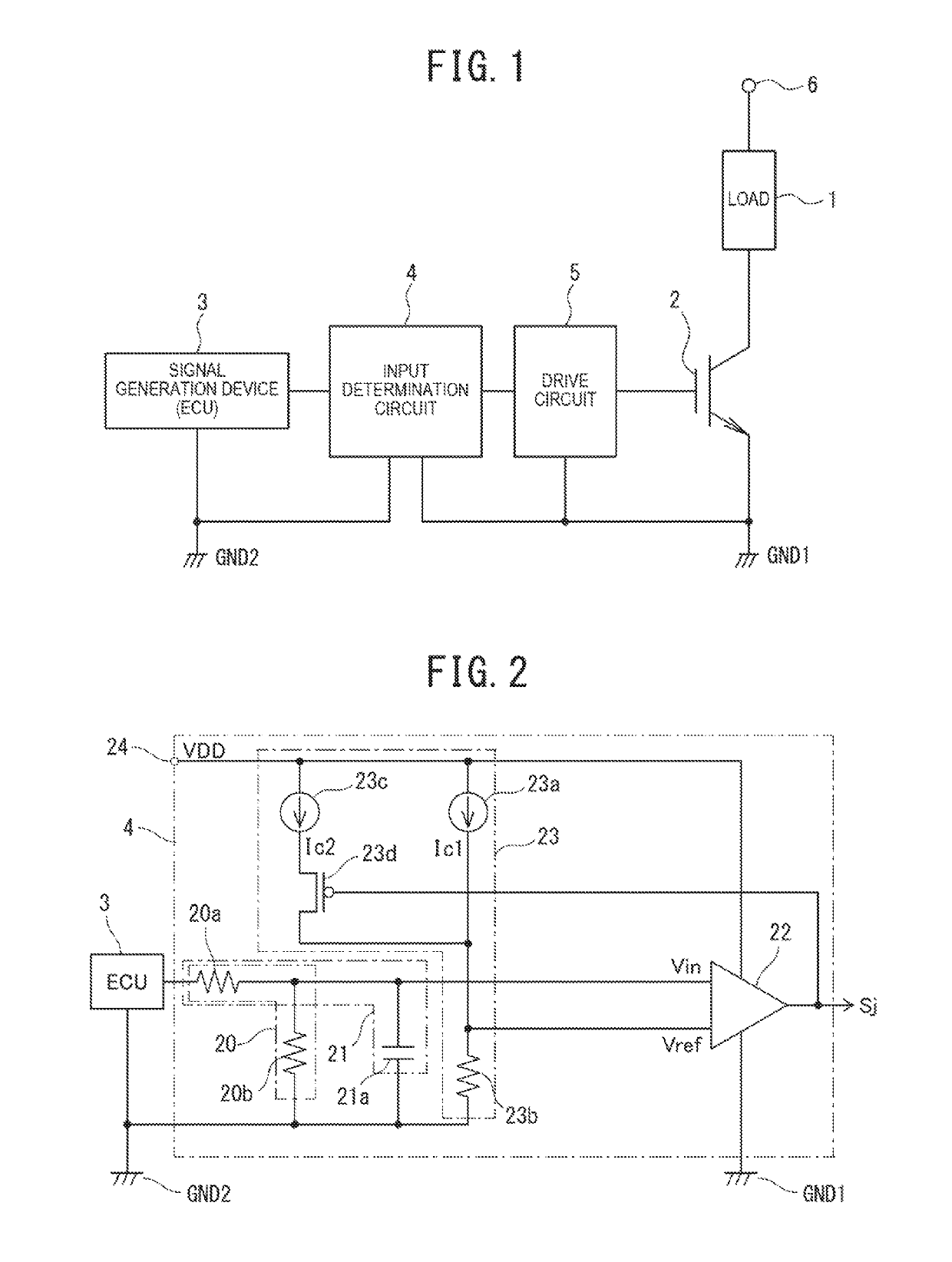
[0020]Hereinafter, a semiconductor device including an input determination circuit in accordance with the present invention will be described using FIG. 1.

[0021]The semiconductor device according to the first embodiment of the present invention is used in, for example, an igniter that drives an inductive load of an ignition coil. The semiconductor device includes an IGBT 2 that drives an inductive load 1. The semiconductor device also includes a signal generation device 3 that outputs a signal for turning the IGBT 2 on and off, an input determination circuit 4 that determines a voltage level of an input signal output from the signal generation device 3 to recognize the ON / OFF state of the input signal, and a drive circuit 5 that controls and drives the IGBT 2 based on a determination output from the input determination circuit 4.

[0022]The collector, emitter, and gate of the IGBT 2 are connected to a DC power supply terminal 6 via the inductive load 1, a ground GND1 that is set at a...

second embodiment

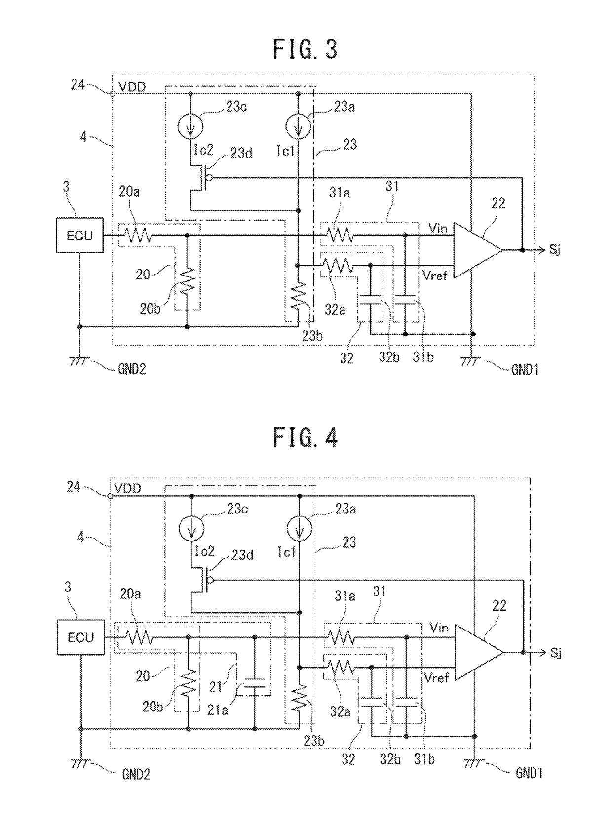
[0050]Next, an input determination circuit 4 according to the present invention will be described using FIG. 3.

[0051]The second embodiment is an embodiment in which the first low pass filter based on the second reference potential in the afore-described first embodiment is omitted, and, in place of the first low pass filter, low pass filters based on a first reference potential that serves as a reference potential for a comparator are added.

[0052]That is, in the second embodiment, the input determination circuit 4 is configured in such a way that, as illustrated in FIG. 3, the capacitor 21a composing the first low pass filter 21 in the first embodiment is omitted, and, in place of the first low pass filter 21, a second low pass filter 31 and a third low pass filter 32 are added immediately before an input voltage terminal and reference voltage terminal of a comparator 22, respectively.

[0053]Since the other configuration is the same as the configuration of the afore-described first e...

third embodiment

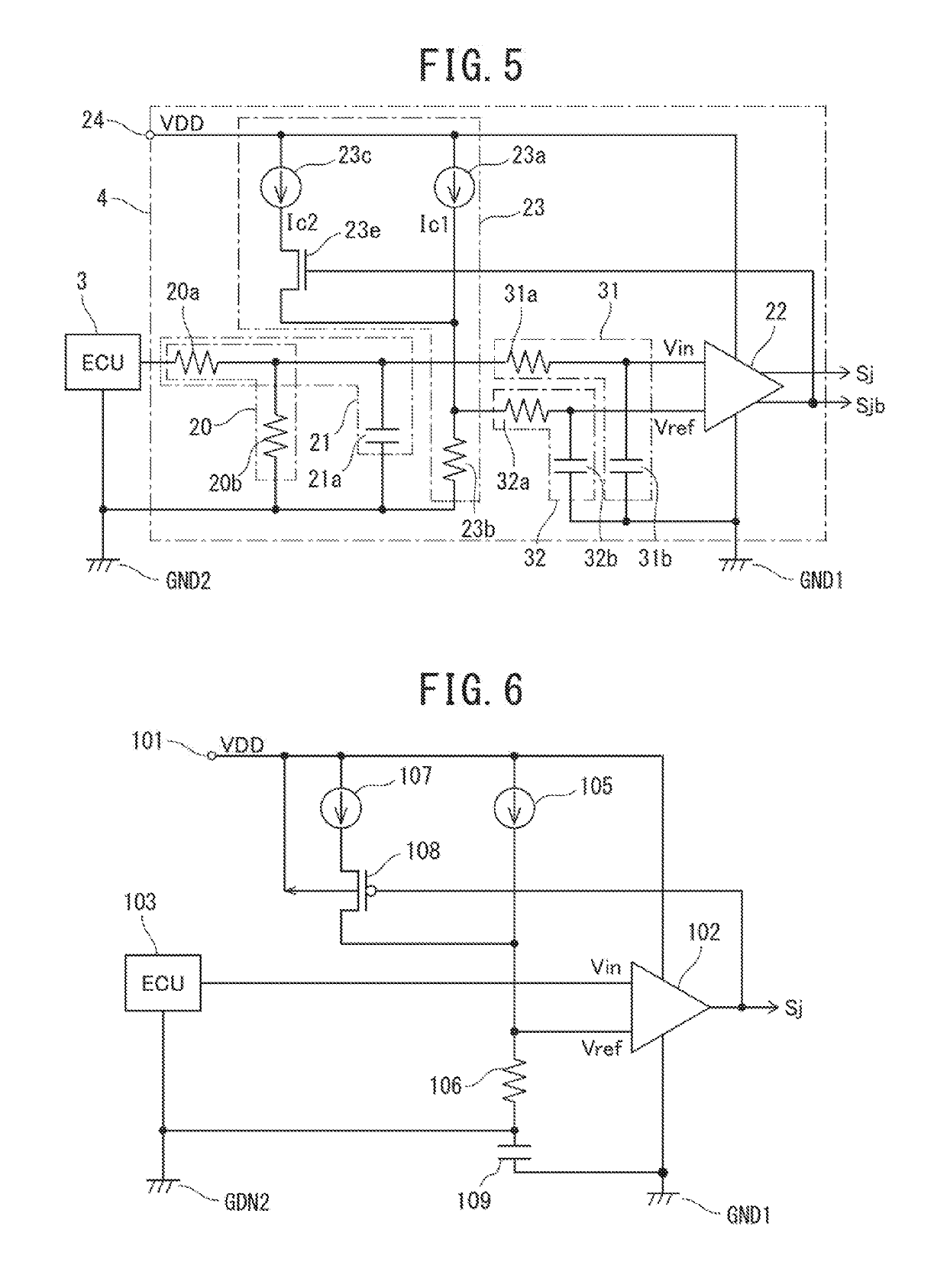
[0058]Next, an input determination circuit according to the present invention will be described using FIG. 4.

[0059]The third embodiment is an embodiment in which the first low pass filter in the afore-described first embodiment and the second low pass filter and the third low pass filter in the afore-described second embodiment are all added to the input determination circuit.

[0060]That is, in the third embodiment, as illustrated in FIG. 4, a first low pass filter 21 is connected between an input voltage system on the input side, which is close to a signal generation device 3, of an input determination circuit 4 and a ground GND2 having a second reference potential G2.

[0061]In addition, a second low pass filter 31 is connected between the input voltage system on the input side of a comparator 22 in the input determination circuit 4 and a ground GND1 having a first reference potential G1.

[0062]Furthermore, a third low pass filter 32 is connected between a reference voltage system on ...


PUM


Abstract

A semiconductor device includes an input determination circuit. The input determination circuit includes: a comparator that is driven based on a first reference potential and includes an input voltage terminal and a reference voltage terminal; a reference voltage generation circuit that inputs a reference voltage that is generated from a connection point between a constant current source and a resistor to the reference voltage terminal of the comparator, the constant current source and the resistor being interposed between a second reference potential that is separated from the first reference potential and a third potential that is higher than the first reference potential and the second reference potential; and a first low pass filter that is interposed between a signal input system that is connected to the input voltage terminal of the comparator and the second reference potential.

Description

REFERENCE[0001]This application claims benefit of priority under 35 USC 119 based on Japanese Patent Application No. 2016-141527 filed on Jul. 19, 2016, the entire contents of which are incorporated by reference herein.TECHNICAL FIELD[0002]The present invention relates to a semiconductor device including an input determination circuit for determining an input signal level.BACKGROUND ART[0003]In general, a semiconductor device that drives a semiconductor switching element based on an input signal is provided with an input determination circuit that includes a comparator for determining an input signal voltage level. In addition, when a power switch capable of flowing a large current therethrough, which is represented by an insulated gate bipolar transistor (hereinafter, referred to as an IGBT), is driven, there is a case in which, since a minute resistance component in wiring and the like serving as a current path may not be ignored and, for example, the potential of a ground in the ...

Claims


Application Information

Patent Timeline
Patent Type & Authority Patents(United States)
IPC IPC(8): H03K5/153
CPCH03K5/084H03K5/153H03K17/30
Inventor ABE, YUYAKOHAMA, TAKANORI
Owner FUJI ELECTRIC CO LTD
Why Eureka
Try Eureka