Two-dimensional photonic crystal surface emitting laser and method of manufacturing the same

a photonic crystal surface and laser technology, applied in the field of semiconductor lasers, can solve the problems of affecting the laser light wave front, difficult to reduce the spot area, and no semiconductor laser currently in practical use has reached this output, etc., to achieve a larger output power and enhance the interference effect

Active Publication Date: 2019-10-29
KYOTO UNIV +3
View PDF32 Cites 1 Cited by
  • Summary
  • Abstract
  • Description
  • Claims
  • Application Information

AI Technical Summary

Benefits of technology

[0029]According to the present invention, it is possible to further enhance an interference effect in a modified refractive index region pair and to obtain laser light with a larger output power.

Problems solved by technology

However, none of the semiconductor lasers currently in practical use has reached this output for the reasons described below.
However, in the semiconductor lasers, as the emission area is increased, laser oscillation occurs in many modes, resulting in disturbed wave front of the laser light.
With the disturbed wave front of the laser light, it is difficult to reduce the spot area even if the light is condensed by using an optical system.
For this reason, it is difficult for the semiconductor laser currently in practical use to obtain a high light output while reducing the spot area.

Method used


Image

  • Two-dimensional photonic crystal surface emitting laser and method of manufacturing the same
  • Two-dimensional photonic crystal surface emitting laser and method of manufacturing the same
  • Two-dimensional photonic crystal surface emitting laser and method of manufacturing the same

Examples


Embodiment Construction

[0049]An embodiment of a two-dimensional photonic crystal surface emitting laser according to the present invention will be described with reference to FIGS. 1 to 19.

[0050](1) Configuration of Two-Dimensional Photonic Crystal Surface Emitting Laser According to the Present Embodiment

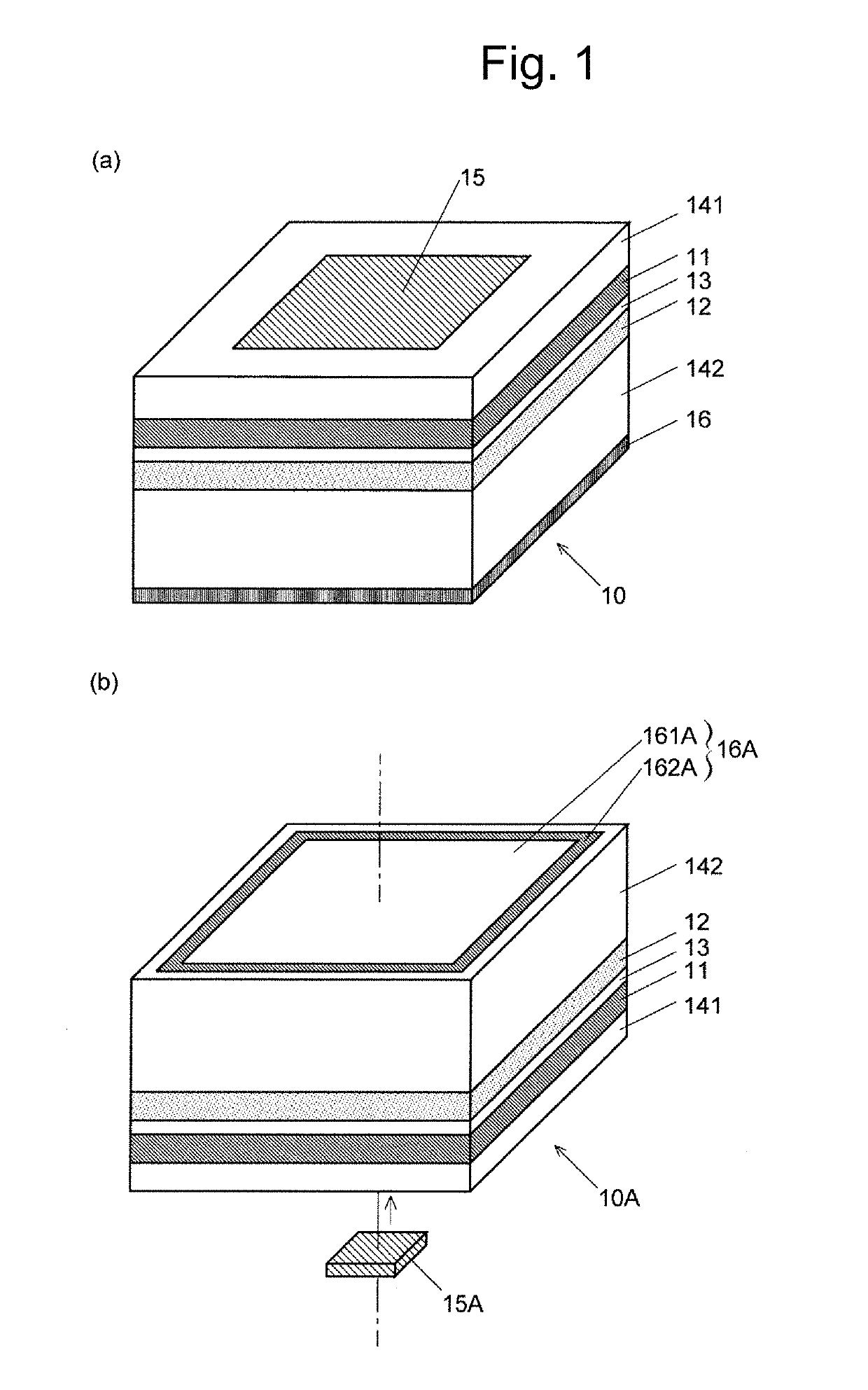
[0051]As illustrated in FIG. 1(a), the two-dimensional photonic crystal surface emitting laser 10 according to this embodiment is configured to include a first electrode 15, a first cladding layer 141, an active layer 11, a spacer layer 13, a two-dimensional photonic crystal layer 12, a second cladding layer 142, and a second electrode 16, which are stacked in this order. However, the order of the active layer 11 and the two-dimensional photonic crystal layer 12 may be reversed from those described above. In FIG. 1(a), for the convenience, the first electrode 15 is illustrated as an upper side, and the second electrode 16 is illustrated as a lower side. However, the orientation of the two-dimensional pho...


PUM


Abstract

A two-dimensional photonic crystal surface emitting laser has, in a plate-shaped base body, a two-dimensional photonic crystal layer in which modified refractive index region pairs are periodically arranged and an active layer provided on one side of the base body, each of the modified refractive index region pairs including a first modified refractive index region and a second modified refractive index region having refractive indexes different from a refractive index of the base body, wherein an area of a planar shape of the first modified refractive index region is larger than or equal to an area of a planar shape of the second modified refractive index region, and a thickness of the first modified refractive index region is smaller than a thickness of the second modified refractive index region.

Description

TECHNICAL FIELD[0001]The present invention relates to a semiconductor laser, and more particularly to a two-dimensional photonic crystal surface emitting laser for amplifying light by using a two-dimensional photonic crystal and a method of manufacturing the two-dimensional photonic crystal surface emitting laser.BACKGROUND ART[0002]Semiconductor lasers have many advantages such as a small size, a low price, low power consumption, and a long life. Due to those advantages, the semiconductor lasers have been widely used in a wide range of fields such as light sources for optical recording, light sources for communication, laser displays, laser printers, and laser pointers. In the field of laser machining, a laser having an optical output exceeding at least 1 W is required. However, none of the semiconductor lasers currently in practical use has reached this output for the reasons described below. Consequently, in the current situation, instead of semiconductor lasers, gas lasers such ...

Claims


Application Information

Patent Timeline
Patent Type & Authority Patents(United States)
IPC IPC(8): H01S5/00H01S5/042H01S5/343H01S5/18H01S5/20H01S5/183H01S5/10H01S5/323H01S5/185
CPCH01S5/3432H01S5/105H01S5/183H01S5/18H01S5/204H01S5/0425H01S2301/17H01S5/323H01S5/34313H01S5/2027H01S5/04253H01S5/04254H01S5/04256H01S5/11H01S5/185
Inventor NODA, SUSUMUTANAKA, YOSHINORIDE ZOYSA, MENAKA
Owner KYOTO UNIV
Why Eureka
Try Eureka