
Semiconductor device and semiconductor device manufacturing method

a semiconductor and semiconductor technology, applied in the field of semiconductor devices, can solve the problems of diodes degrading reliability similarly to p-n diodes, increasing forward bias of p-n diodes, and reducing reliability, so as to reduce stress test time, and suppress transistor characteristics caused by stress test

Active Publication Date: 2019-11-12
MITSUBISHI ELECTRIC CORP
View PDF23 Cites 0 Cited by
  • Summary
  • Abstract
  • Description
  • Claims
  • Application Information

AI Technical Summary

Benefits of technology

The present invention provides a structure for reducing stress current during a stress test of a p-n junction by placing a separate second electrode that is in contact with the second well region outside the active region. This results in smaller heat generated in the active region, allowing a higher current to be applied in the stress test and reducing the time required for the test. Additionally, the formation of stacking faults in the active region during the stress test is suppressed, resulting in less variation in transistor characteristics and reducing the time required for the test.

Problems solved by technology

It can be considered that increase in the forward bias of the p-n diode occurs because the triangular stacking faults obstruct the current flow.
Such increase in the forward bias may degrade the reliability.
In the MOSFET structure, a parasitic p-n diode (body diode) is interposed between a source and a drain, and application of a forward current to this body diode degrades the reliability similarly as the p-n diode.
However, as pointed out by Patent Document 1, the external installation of a diode increases the number of parts included in a device.
An excess current to finish the test for a short period of time may damage a chip or test equipment through excess generation of heat in a diode element.
Conversely, reduction in current requires a longer time to test, which consequently causes practical problems including increase in the chip cost.

Method used


Image

  • Semiconductor device and semiconductor device manufacturing method
  • Semiconductor device and semiconductor device manufacturing method
  • Semiconductor device and semiconductor device manufacturing method

Examples


embodiment 1

[0037](Structure)

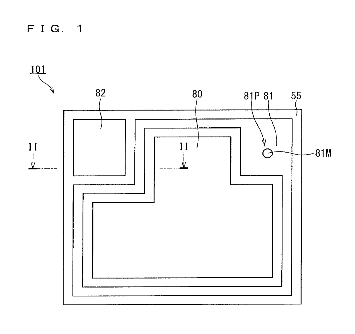
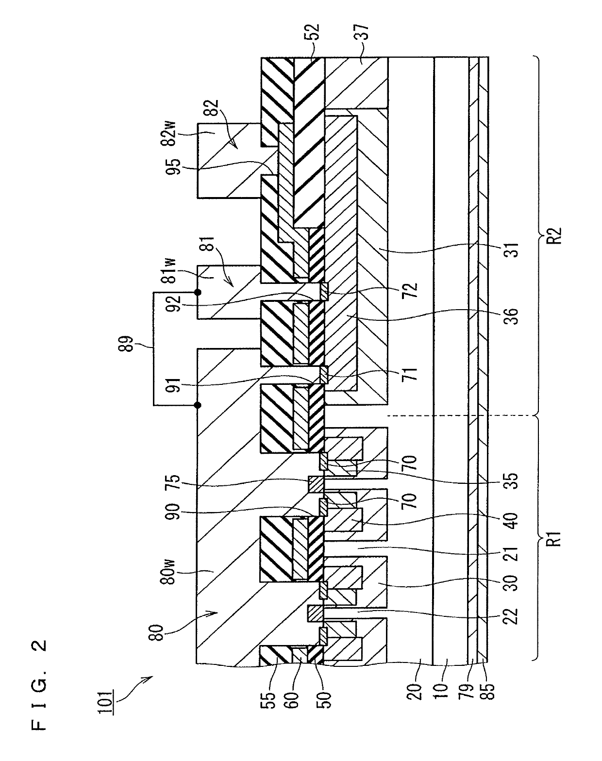
[0038]A structure of a MOSFET 101 (semiconductor device) according to Embodiment 1 will be described with reference to FIGS. 1 and 2. The MOSFET 101 incorporates an SBD, which will be later described in detail.

[0039]The MOSFET 101 includes a substrate 10 (semiconductor substrate) having n-type conductivity (first conductivity type), a semiconductor layer on the substrate 10, a gate insulating film 50, a field insulating film 52, an interlayer insulating film 55, a source electrode 80 (first electrode), a test electrode 81 (second electrode), a gate electrode 82, an ohmic electrode 79, and a drain electrode 85 (third electrode). The semiconductor layer includes a drift layer 20 having n-type conductivity, a plurality of well regions 30 (first well regions) having p-type conductivity (a second conductivity type different from the first conductivity type), a well region 31 (second well region) having p-type conductivity, source regions 40 having n-type conductivity, an...

embodiment 2

[0099]With reference to FIG. 7, the field insulating film 52 extends to a position closer to the active region R1 in a MOSFET 102 (semiconductor device) according to Embodiment 2 than that of the MOSFET 101 (FIG. 2). In other words, a boundary between the field insulating film 52 and the gate insulating film 50 is positioned closer to the active region R1 than the contact holes 91 and 92 are. As a result, the contact holes 91 and 92 penetrate not only the interlayer insulating film 55 but also the field insulating film 52. Thus, the ohmic contact parts 71 and 72 are disposed in the contact holes 91 and 92 provided in the field insulating film 52, respectively.

[0100]Since the structures other than above are almost the same as those according to Embodiment 1, the same or corresponding constituent elements are denoted by the same reference numerals and the description thereof will not be repeated.

[0101]During a switching operation of the MOSFET 102, the potential of the well region 31 ...

embodiment 3

[0105]With reference to FIG. 8, a MOSFET 103 (semiconductor device) according to Embodiment 3 does not include the contact hole 91 unlike the MOSFET 102 (FIG. 7). Thus, the source electrode 80 and the well region 31 are separated by the insulating films. In a practical use of the MOSFET 103 according to Embodiment 3, the wiring part 89 needs to short-circuit the source electrode 80 and the test electrode 81 after application of the stress current to prevent the potential of the well region 31 from being in a floating state.

[0106]Since the structures other than above are almost the same as those according to Embodiment 2, the same or corresponding constituent elements are denoted by the same reference numerals and the description thereof will not be repeated.

[0107]According to Embodiment 3, the current to be applied by the test electrode 81 in the stress test can be prevented from leaking to the active region R1 through a current path passing through the contact hole 91. Accordingly,...


PUM


Abstract

A drift layer is made of a wide bandgap semiconductor. First well regions are formed on the drift layer. A source region is formed on each of the first well regions. A gate insulating film is formed on the first well regions. A first electrode is in contact with the source regions, and has diode characteristics allowing unipolar conduction to the drift layer between the first well regions. A second well region is formed on the drift layer. A second electrode is in contact with the second well region, and separated from a gate electrode and the first electrode.

Description

TECHNICAL FIELD[0001]The present invention relates to a semiconductor device and a method for manufacturing the same, and particularly to a semiconductor device using a wide bandgap semiconductor and a method for manufacturing the same.BACKGROUND ART[0002]It is known that continuous application of a forward current to a p-n diode using silicon carbide (SiC) increases a forward bias (for example, see Non-Patent Document 1 below). This occurs because recombined energy obtained when minority carriers injected through the p-n diode are recombined with majority carriers causes the triangular stacking faults (may also be referred to as “Shockley-type stacking faults”), which are plane defects, to extend into crystals from basal plane dislocations, etc. in a silicon carbide substrate as an origin (for example, see Non-Patent Document 2 below). It can be considered that increase in the forward bias of the p-n diode occurs because the triangular stacking faults obstruct the current flow. Suc...

Claims


Application Information

Patent Timeline
Patent Type & Authority Patents(United States)
IPC IPC(8): H01L29/06H01L29/16H01L29/66H01L29/78H01L29/47
CPCH01L29/0649H01L29/66068H01L29/47H01L29/1608H01L29/7815H01L29/872H01L22/14H01L22/32H01L29/7805H01L29/7806H01L29/0615
Inventor SADAMATSU, KOJIHINO, SHIRO
Owner MITSUBISHI ELECTRIC CORP
Learn More