Method of manufacturing liquid crystal display device and manufacturing system for liquid crystal display device

a manufacturing system and liquid crystal display technology, applied in non-linear optics, instruments, optics, etc., can solve the problems of inability to accurately measure the gap, the deformation of the columnar spacer may be hardly, and the spacer beads may adversely be arranged, etc., to achieve the effect of high yield ra

Active Publication Date: 2020-04-14
TRIVALE TECH
View PDF13 Cites 0 Cited by
  • Summary
  • Abstract
  • Description
  • Claims
  • Application Information

AI Technical Summary

Benefits of technology

[0008]The present invention is made in order to solve the problems as described above, and has an object to provide a method of manufacturing a liquid crystal display device and a manufacturing system for a liquid crystal display device, in which the liquid crystal display device can be manufactured with a high yield rate even when a height of at least one columnar spacer has dispersion.
[0009]A method of manufacturing a liquid crystal display device according to the present invention is a method of manufacturing a liquid crystal display device including a liquid crystal panel having a first substrate and a second substrate that oppose each other through intermediation of a gap, at least one columnar spacer for retaining the gap, and a liquid crystal layer inside the gap. The at least one columnar spacer is formed on the first substrate. A height of the at least one columnar spacer is measured. Liquid crystal is dropped on any one of the first substrate and the second substrate with an amount of the liquid crystal that is determined based on a determination function dependent upon the height of the at least one columnar spacer in order to provide the liquid crystal layer. The determination function is provided in advance in consideration of prevention of maldistribution of the liquid crystal layer caused by temperature increase, prevention of generation of air bubbles inside the gap caused by temperature decrease, and satisfaction of an upper limit condition and a lower limit condition for a dimension of the gap required by optical properties of the liquid crystal panel.
[0011]According to the method of manufacturing a liquid crystal display device of the present invention, the determination function for determining the amount of the liquid crystal dependently upon the height of the at least one columnar spacer is provided in advance in consideration of prevention of the maldistribution of the liquid crystal layer caused by temperature increase, prevention of the generation of the air bubbles inside the gap caused by temperature decrease, and satisfaction of the upper limit condition and the lower limit condition for the dimension of the gap required by the optical properties of the liquid crystal panel. With this, even when the height of the at least one columnar spacer has dispersion, it is possible to more accurately prevent the maldistribution of the liquid crystal layer caused by temperature increase, prevent the generation of the air bubbles inside the gap caused by temperature decrease, and satisfy the upper limit condition and the lower limit condition for the dimension of the gap required by the optical properties of the liquid crystal panel. That is, even when the height of the at least one columnar spacer has dispersion, the liquid crystal display device can be manufactured with a high yield rate.
[0012]According to the manufacturing system for a liquid crystal display device of the present invention, in a case where the quality of the first substrate on which the at least one columnar spacer is provided is determined as nondefective, the amount of the liquid crystal is determined. With this, the first substrate, of which quality is determined as “defective,” can be removed from a manufacturing process. Thus, even when the height of the at least one columnar spacer has dispersion, the liquid crystal display device can be manufactured with a high yield rate.

Problems solved by technology

The spacer beads are randomly dispersed on the substrates, and thus the spacer beads may adversely be arranged even in the pixel portions in some cases.
Further, under low temperature, the elastic deformation of the columnar spacers may hardly follow thermal contraction of the liquid crystal.
Thus, when the amount of the liquid crystal is determined in consideration of prevention the generation of the high-temperature gap unevenness and the generation of the low-temperature bubbling alone, the dimension of the gap may become inappropriate.

Method used


Image

  • Method of manufacturing liquid crystal display device and manufacturing system for liquid crystal display device
  • Method of manufacturing liquid crystal display device and manufacturing system for liquid crystal display device
  • Method of manufacturing liquid crystal display device and manufacturing system for liquid crystal display device

Examples


first preferred embodiment

[0047](Configuration of Liquid Crystal Panel)

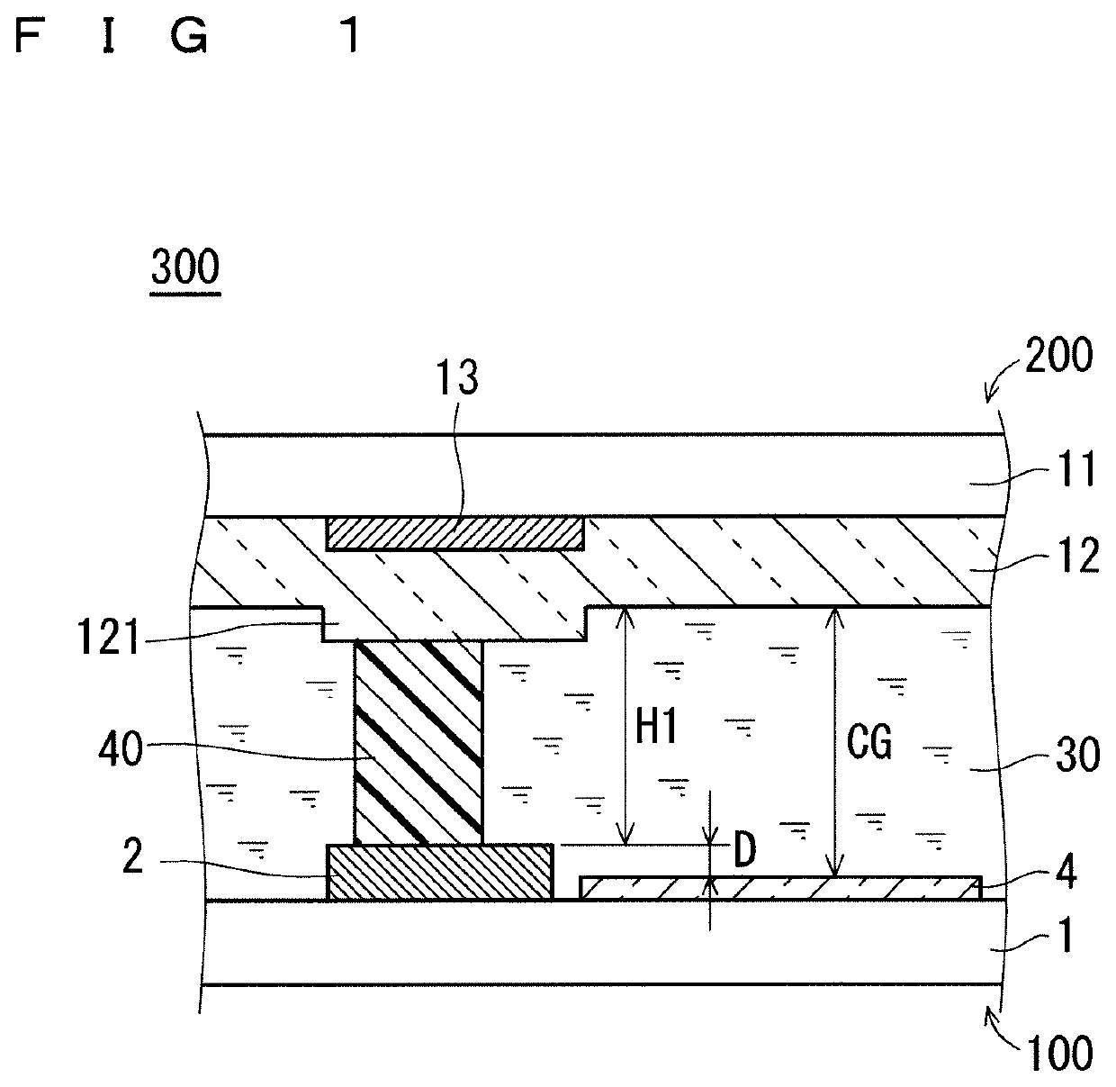
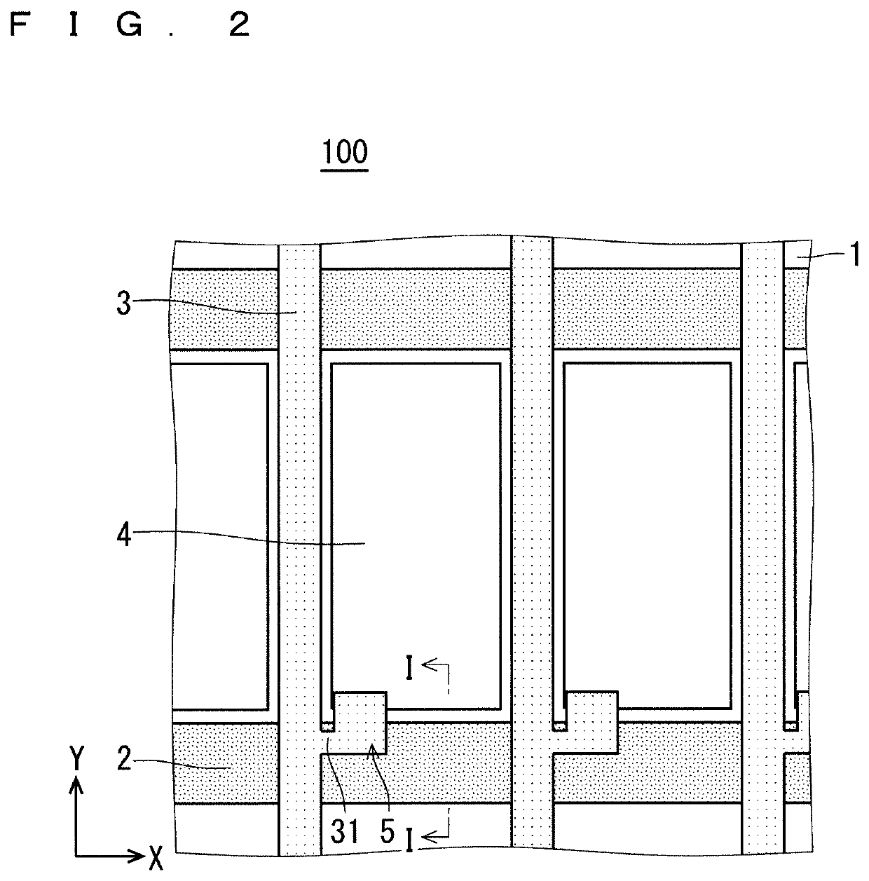
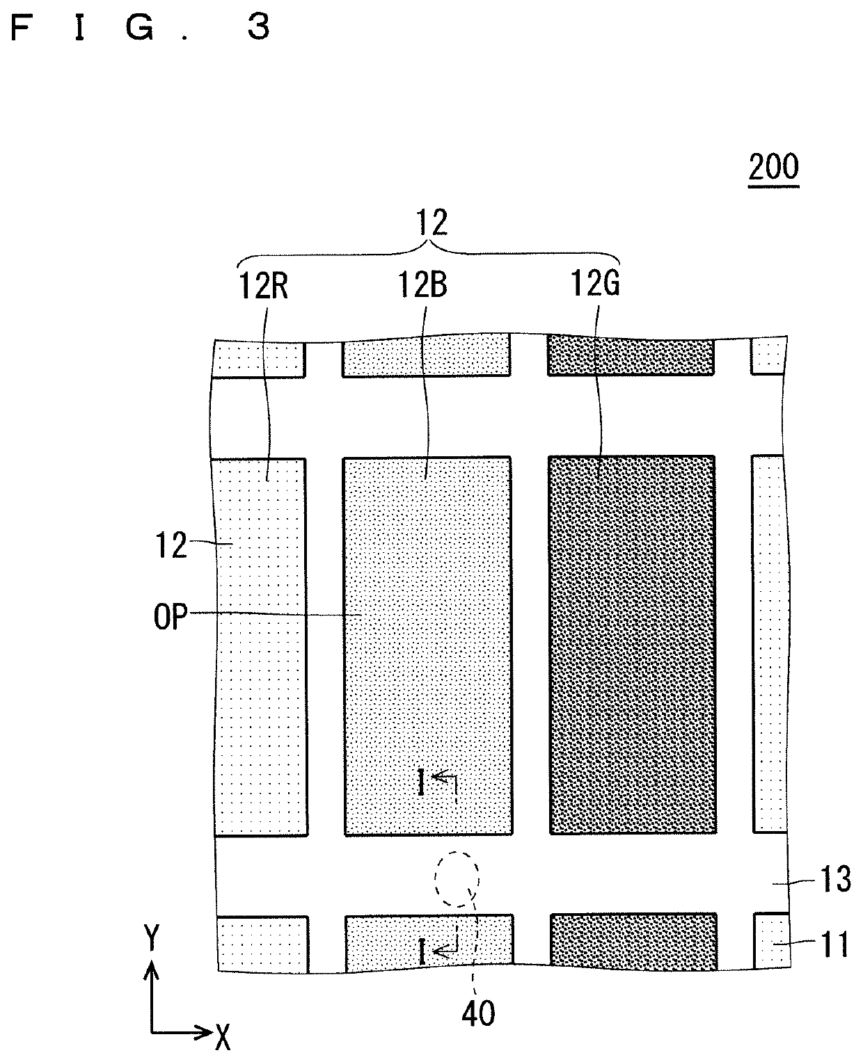
[0048]FIG. 1 is a view for schematically illustrating configuration of a liquid crystal panel 300 of a liquid crystal display device according to this preferred embodiment, specifically, a partial sectional view taken along the line I-I of FIG. 2 and FIG. 3. FIG. 2 is a partial plan view for schematically illustrating configuration of the TFT substrate 100 of the liquid crystal panel 300. FIG. 3 is a partial plan view for schematically illustrating configuration of the CF substrate 200 of the liquid crystal panel 300. The liquid crystal panel 300 includes the CF substrate 200 (first substrate) and the TFT substrate 100 (second substrate) that oppose each other through intermediation of the cell gap CG, the columnar spacers 40 for retaining the cell gap CG, and the liquid crystal layer 30 inside the cell gap CG.

[0049]The TFT substrate 100 includes a transparent substrate 1, gate wirings 2, source wirings 3, a pixel electrode 4, and a TFT 5...

second preferred embodiment

[0090]In the first preferred embodiment, as illustrated in FIG. 5, description is given to the case where one type of columnar spacer is used. In this preferred embodiment, description is given to the case of a dual spacer structure as illustrated in FIG. 8. In the dual spacer structure, the high-temperature gap unevenness is mainly related to the columnar spacer 40, and the low-temperature bubbling is mainly related to the sub-columnar spacer 41.

[0091]FIG. 14 is a graph for showing an example of a method of calculating the amount of the liquid crystal according to this preferred embodiment. In FIG. 14, for the purpose of obtaining a comprehensive graph that corresponds to the dual spacer structure, a horizontal axis is represented with use of the height H0 of the columnar spacer 40 (FIG. 8). The height H0 of the columnar spacer 40 is converted into a height of the sub-columnar spacer 41 (FIG. 8) by subtracting a dimensional difference provided at the time of designing. The dimensio...

third preferred embodiment

[0100]FIG. 16 is a graph for showing an example of a method of calculating the amount of the liquid crystal according to this preferred embodiment. In the height range R3, as a determination function Q3, an intermediate value of the cell-gap upper limit LU and the cell-gap lower limit LL is used. In the height range R1 and the height range R2, as the determination function Q3, values that are different from the above-mentioned intermediate value are used. Specifically, in the height range R1, in order to preferentially arrange a dispersion upper limit DU3 not to exceed the high-temperature limit BH, such a linear function is used that an allowance corresponding to the dispersion of 0.05 μm is secured with respect to the high-temperature limit BH. In the height range R2, in order to preferentially arrange a dispersion lower limit DL3 not to exceed the low-temperature limit BL, such a linear function is used that an allowance corresponding to the dispersion of 0.05 μm is secured with ...


PUM

PropertyMeasurementUnit
height H1aaaaaaaaaa
heightaaaaaaaaaa
heightaaaaaaaaaa

Abstract

At least one columnar spacer is formed on a first substrate. A height of the columnar spacer is measured. In order to provide a liquid crystal layer, liquid crystal is dropped onto any one of the first substrate and a second substrate with an amount of the liquid crystal determined based on a determination function dependent upon the height of the columnar spacer. The determination function is provided in advance in consideration of prevention of maldistribution the liquid crystal layer caused by temperature increase, prevention of generation of air bubbles inside a gap caused by temperature decrease, and satisfaction of an upper limit condition and a lower limit condition for a dimension of the gap required by optical properties of a liquid crystal panel.

Description

BACKGROUND OF THE INVENTIONField of the Invention[0001]The present invention relates to a method of manufacturing a liquid crystal display device and a manufacturing system for a liquid crystal display device, and more particularly, to a method of manufacturing a liquid crystal display device including at least one columnar spacer for retaining a gap between substrates and a manufacturing system for the liquid crystal display device.Description of the Background Art[0002]A liquid crystal display device includes a liquid crystal panel in which an image is displayed, and further includes a backlight in a case of a transmission type or a semi-transmission type. The liquid crystal panel includes a pair of substrates that oppose each other through intermediation of a liquid crystal layer. Typically, one substrate is an active matrix substrate, that is, a thin film transistor (TFT) substrate. Another substrate is a color filter (CF) substrate. In the TFT substrate, wirings are arranged in...

Claims


Application Information

Patent Timeline
Patent Type & Authority Patents(United States)
IPC IPC(8): G02F1/1341G02F1/13G02F1/1339
CPCG02F1/1339G02F1/1341G02F1/1303G02F1/1309G02F1/13394G02F2001/13415G02F2001/13398G02F1/13398G02F1/13415
Inventor TAMATANI, AKIRA
Owner TRIVALE TECH
Why Eureka
Try Eureka