Display device, electronic device, and operation method thereof

a technology of electronic devices and display devices, applied in the direction of instruments, computing, electric digital data processing, etc., can solve the problem of large power consumption of sensing, and achieve the effect of low power consumption

Active Publication Date: 2020-04-14
SEMICON ENERGY LAB CO LTD
View PDF42 Cites 1 Cited by
  • Summary
  • Abstract
  • Description
  • Claims
  • Application Information

AI Technical Summary

Benefits of technology

[0011]Another object of one embodiment of the present invention is to provide a display device with low power consumption. Another object of one embodiment of the present invention is to provide a novel driving method for touch sensing.
[0016](4) Another embodiment of the present invention is a method for operating an electronic device including a display device and a touch sensor. The display device includes a display portion and an illuminance sensor. The illuminance sensor has a function of measuring the illuminance of external light to divide the display portion into a first region which is not shaded and a second region which is shaded. The luminance of an image displayed in the first region of the display portion is increased. No image is displayed in the second region of the display portion, or the luminance of an image displayed in the second region of the display portion is reduced.
[0023]According to another embodiment of the present invention, a display device with low power consumption can be provided. According to another embodiment of the present invention, a novel driving method for touch sensing can be provided.

Problems solved by technology

This is because the writing of the image data causes a noise.
Therefore, a large amount of power might be consumed for the sensing.

Method used


Image

  • Display device, electronic device, and operation method thereof
  • Display device, electronic device, and operation method thereof
  • Display device, electronic device, and operation method thereof

Examples


embodiment 1

[0059]In this embodiment, a display device, a touch sensor portion, and an operation method thereof will be described.

Configuration Example

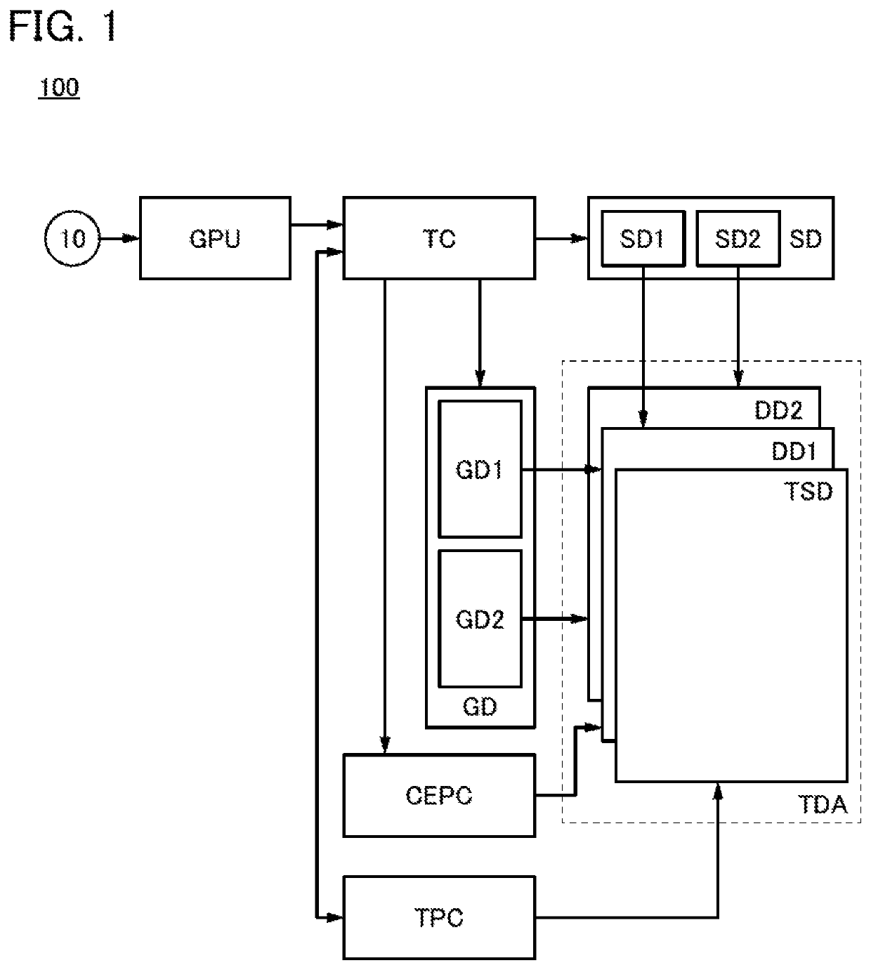
[0060]FIG. 1 is a block diagram illustrating a configuration example of an electronic device described in this embodiment.

[0061]In this embodiment, an electronic device 100 is a hybrid display device in which a common electrode of a reflective liquid crystal element is also used as a touch sensor electrode of a touch sensor portion and an OS FET is used as a transistor included in a pixel circuit. The electronic device 100 includes a graphics processing unit GPU, a timing controller TC, a common electrode potential setting circuit CEPC, a touch panel controller TPC, a gate driver portion GD, a source driver portion SD, and a touch sensor display portion TDA.

[0062]The gate driver portion GD includes a first gate driver GD1 and a second gate driver GD2. The source driver portion SD includes a first source driver SD1 and a second source driver SD2. ...

embodiment 2

[0109]In this embodiment, a display device and a touch sensor portion which are different from those in Embodiment 1 and an operation method thereof will be described.

configuration example 1

[0110]FIG. 6 is a block diagram illustrating a configuration example of an electronic device described in this embodiment.

[0111]An electronic device 101 is an electronic device which includes a first display device DD1 including a reflective liquid crystal element (or a transmissive liquid crystal element; hereinafter, the general term “liquid crystal element” will be used) and in which an OS FET is used as a transistor included in a pixel circuit. Note that unlike in Embodiment 1, a common electrode of the liquid crystal element and a touch sensor electrode in a touch sensor portion are separately provided. The electronic device 101 includes a graphics processing unit GPU, a timing controller TC, a touch panel controller TPC, a first gate driver GD1, a first source driver SD1, and a touch sensor display portion TDA.

[0112]The electronic device 101 has a configuration corresponding to that of the electronic device 100 in Embodiment 1 which does not include the second display device D...


PUM

PropertyMeasurementUnit
drive frequencyaaaaaaaaaa
frequencyaaaaaaaaaa

Abstract

A method for operating an electronic device with lower power consumption is provided. The electronic device includes a display device and a touch sensor. In the case where the touch sensor senses no touch, the touch sensor is brought into a resting state or operated so as to perform a sensing operation at a reduced drive frequency. Also in the case where the touch sensor constantly senses touches and an image on the display device is not changed, the touch sensor is brought into the resting state or operated so as to perform the sensing operation at a reduced drive frequency.

Description

BACKGROUND OF THE INVENTION1. Field of the Invention[0001]One embodiment of the present invention relates to a display device, an electronic device, or an operation method thereof.[0002]Note that one embodiment of the present invention is not limited to the above technical field. The technical field of the invention disclosed in this specification and the like relates to an object, a method, or a manufacturing method. Furthermore, one embodiment of the present invention relates to a process, a machine, manufacture, or a composition of matter. Specifically, examples of the technical field of one embodiment of the present invention disclosed in this specification include a semiconductor device, a display device, a liquid crystal display device, a light-emitting device, a power storage device, an imaging device, a memory device, a processor, an electronic device, a method for driving any of them, a method for manufacturing any of them, a method for testing any of them, and a system inc...

Claims


Application Information

Patent Timeline
Patent Type & Authority Patents(United States)
IPC IPC(8): G06F1/3234G06F3/041G02F1/1333G02F1/1343G06F3/0488G06F3/045G06F3/044
CPCG06F1/3262G06F3/045G02F1/13338G06F3/0488G06F3/0412G02F1/1343G06F3/044G06F3/0416G06F3/04166G06F3/0446G06F3/0443G06F3/0445
Inventor IWAKI, YUJIYAMAZAKI, SHUNPEI
Owner SEMICON ENERGY LAB CO LTD
Why Eureka
Try Eureka