Display device, electronic apparatus, and display device manufacturing method

a technology of electronic equipment and display devices, applied in the direction of solid-state devices, organic semiconductor devices, oled structures, etc., can solve the problems of reduced efficiency, light, color mixture, etc., and achieve the effect of reducing leakage curren

Active Publication Date: 2020-04-28
CANON KK
View PDF8 Cites 1 Cited by
  • Summary
  • Abstract
  • Description
  • Claims
  • Application Information

AI Technical Summary

Benefits of technology

[0012]Another aspect of the disclosure provides a display device that includes insulating layers laminated between adjacent organic light emitting elements and has reduced leakage current through an interface between the insulating layers.

Problems solved by technology

As pixels of a display device using organic light emitting elements have become denser in recent years, a problem of leakage current through an organic layer which is provided commonly between adjacent pixels which are close to each other has come to light.
Accordingly, a non-light emitting pixel slightly emits light due to the influence from a light emitting pixel, which causes color mixture or reduction in efficiency.

Method used


Image

  • Display device, electronic apparatus, and display device manufacturing method
  • Display device, electronic apparatus, and display device manufacturing method
  • Display device, electronic apparatus, and display device manufacturing method

Examples


first example embodiment

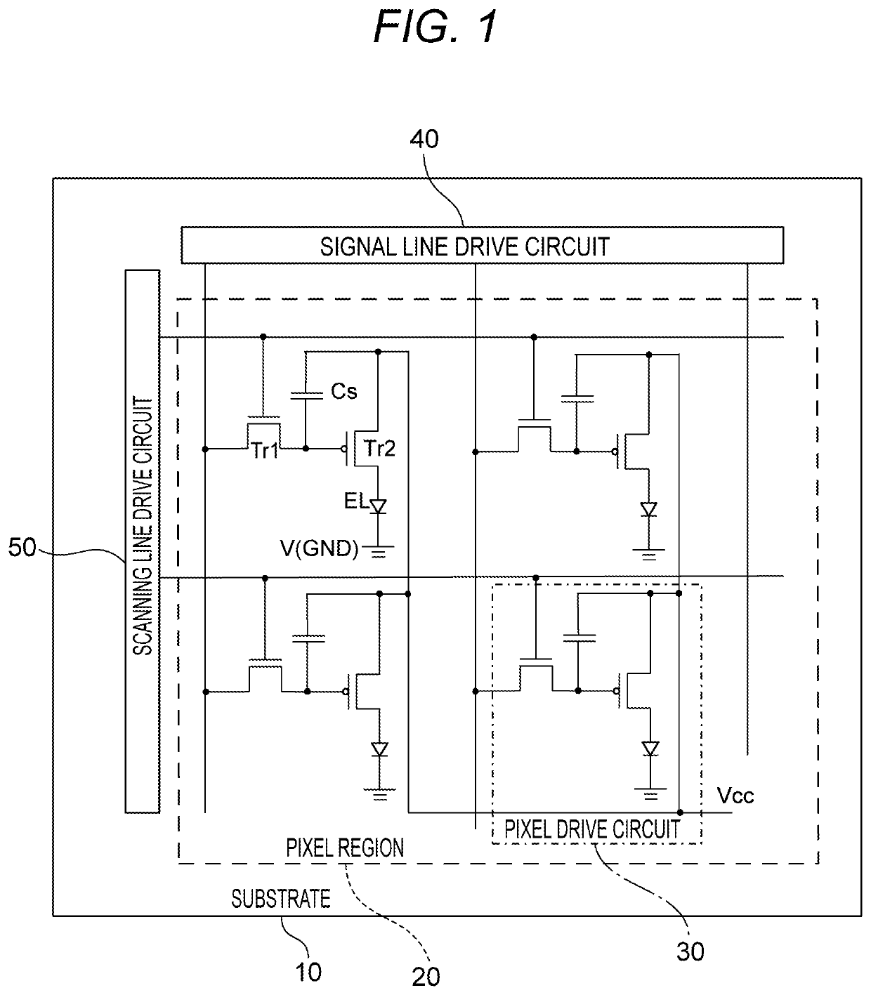
[0037]FIGS. 1 to 8B illustrate the configuration of a display device according to the present embodiment. FIG. 1 is an equivalent circuit diagram of an example of the display device. A plurality of light emitting elements EL are arrayed in a pixel region 20 which is laid out on a substrate 100. Each of the light emitting elements EL corresponds to, for example, a sub-pixel 2 of red, green, or blue. A peripheral circuit region is disposed around the pixel region 20. The peripheral circuit region is provided with, for example, a signal line drive circuit 40 and a scanning line drive circuit 50 which are drivers for video display.

[0038]A plurality of sub-pixels 2 are arranged in the pixel region 20. Each of the sub-pixels 2 includes, for example, a pixel drive circuit 30 and a light emitting element EL. The pixel drive circuit 30 is an active drive circuit which is disposed in a layer lower than a first electrode (described below). The pixel drive circuit 30 includes, for example, a wr...

second example embodiment

[0139]In the present embodiment, only a part that differs from the first embodiment will be described with reference to FIGS. 12 and 13. Description for a configuration, a function, a material, and an effect that are similar to those of the first embodiment will be omitted.

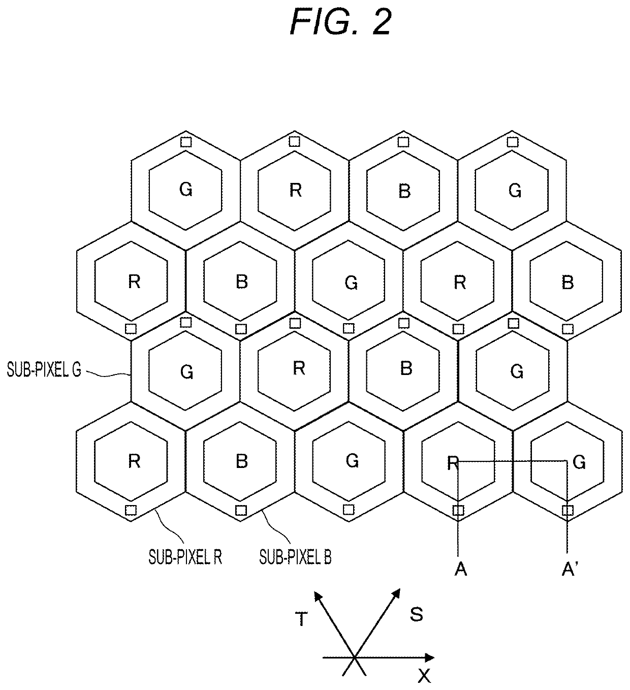
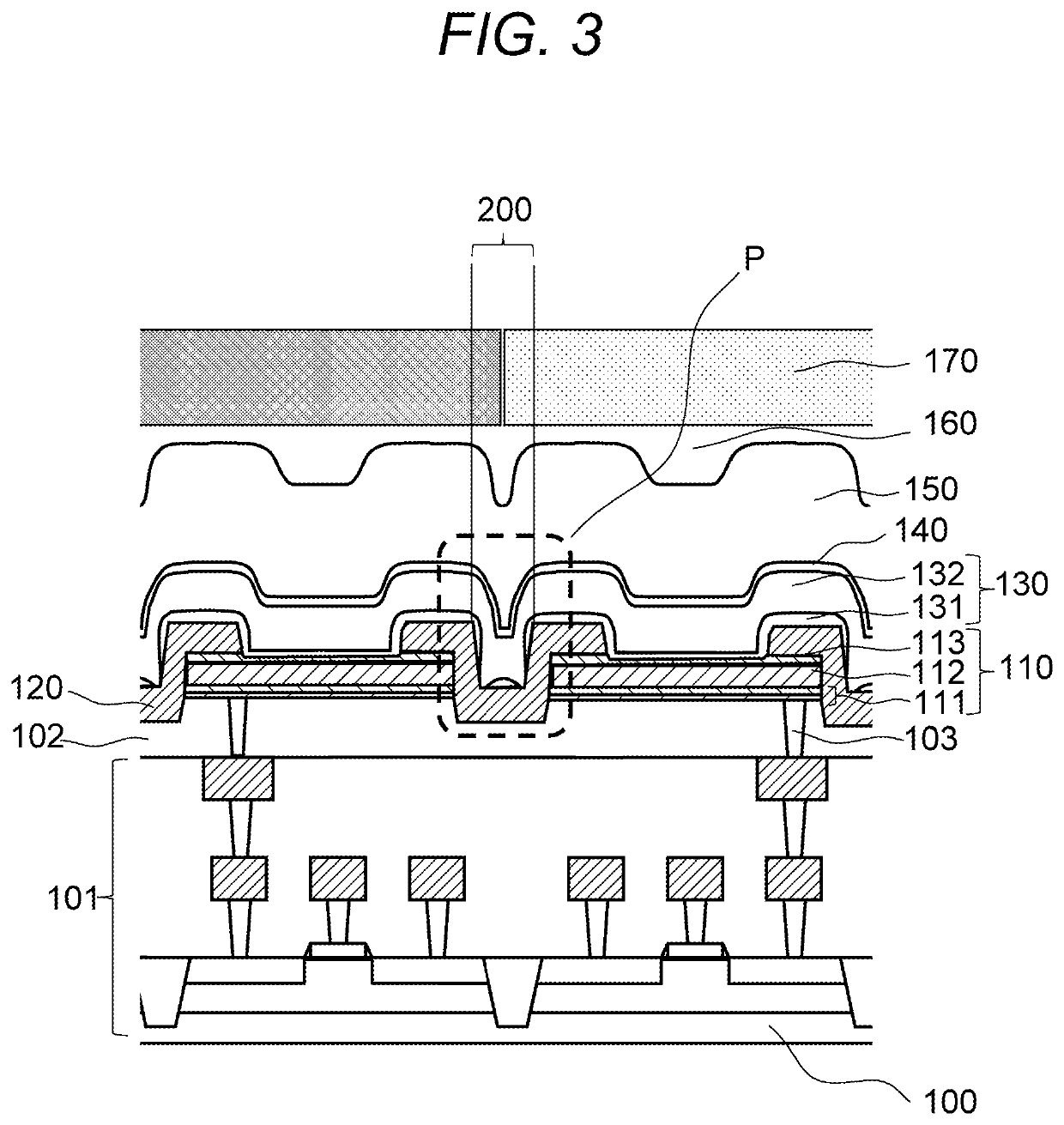
[0140]FIG. 12 is a schematic sectional view of a part corresponding to line A-A′ which extends across two adjacent sub-pixels in FIG. 2 described in the first embodiment. As described above, there are a pixel region and a peripheral circuit region on a substrate 100. A drive circuit layer 101 which includes a pixel circuit is disposed corresponding to each of the regions. The drive circuit layer 101 includes various transistors, a capacitor unit, and a wiring layer. The drive circuit layer may be appropriately provided with a light shielding layer for reducing stray light to the transistors.

[0141]A first insulating layer 102 is disposed over the drive circuit layer 101. Organic light emitting elements as light emi...

third example embodiment

[0152]In the present embodiment, only a part that differs from the first and second embodiments will be described with reference to FIGS. 14 to 19B. Description for a configuration, a function, a material, and an effect that are similar to those of the first embodiment will be omitted.

[0153]FIG. 14 is a schematic sectional view of a part corresponding to line A-A′ which extends across two adjacent sub-pixels in FIG. 2 described in the first embodiment. As illustrated in FIG. 14, each sub-pixel is provided with a first electrode 110. A voltage or a current applied to each first electrode 110 can be independently controlled. A conductive member 115 is disposed between adjacent first electrodes 110.

[0154]A voltage or a current applied to the conductive member 115 can be controlled independently of the first electrodes 110 which are adjacent to the conductive member 115. The conductive member 115 may have a common potential within a display region, or a plurality of conductive members 1...


PUM

PropertyMeasurementUnit
angleaaaaaaaaaa
aspect ratioaaaaaaaaaa

Abstract

An embodiment provides a display device including an insulating layer which is continuous between opposed ends of two adjacent lower electrodes from an upper part of one of the ends to an upper part of the other end, a first organic layer which is disposed over the lower electrodes and the insulating layer, a second organic layer which is disposed over the lower electrodes and the insulating layer with the first organic layer interposed therebetween and includes a light emitting layer, and a second electrode which covers the organic layer. The upper face of the insulating layer includes a recess between the two lower electrodes. The aspect ratio of the recess is 0.5 or more.

Description

BACKGROUND OF THE INVENTIONField of the Invention[0001]The disclosure relates to a display device, an electronic apparatus, and a display device manufacturing method.Description of the Related Art[0002]For example, there is an organic light emitting display device as a display device. An organic light emitting element of the organic light emitting display device generates light by recombination of electrons injected from a cathode with holes injected from an anode in an organic light emitting layer. The generated light is extracted from the cathode side or the anode side.[0003]In an active matrix display device using an organic light emitting element, a pixel drive circuit which includes a drive transistor and a multilayer wiring structure is formed on a substrate, and organic light emitting elements are arrayed on the substrate. As such a display device, there is known a top emission display device which uses a light transmissive conductive material as a cathode. The top emission d...

Claims


Application Information

Patent Timeline
Patent Type & Authority Patents(United States)
IPC IPC(8): H01L27/32H01L51/50H01L51/56H01L51/52
CPCH01L27/3258H01L27/3244H01L51/56H01L51/5012H01L27/3246H01L51/5088H01L51/5056H01L51/5265H01L51/5209H01L27/322H01L27/3218H01L51/5253H01L2251/53H01L2251/558H01L2251/5315H01L27/3272H01L2227/323H01L2924/12044H01L51/5218H10K59/353H10K59/122H10K50/813H10K2102/351H10K50/11H10K50/15H10K50/17H10K59/12H10K59/124H10K71/00H10K50/818H10K50/844H10K50/852H10K59/38H10K59/126H10K59/1201H10K2102/302H10K2102/3026
Inventor UKIGAYA, NOBUTAKA
Owner CANON KK
Why Eureka
Try Eureka