Maskless exposure method, maskless exposure apparatus and method of manufacturing a semiconductor device using the same

a maskless exposure and semiconductor technology, applied in the field of maskless exposure methods, maskless exposure apparatuses, and semiconductor device manufacturing methods, can solve the problems of not being able to precisely focus all spot beams on portions having different heights, increasing the manufacturing cost of photomasks, etc., to improve the resolution of the exposure apparatus, the effect of preventing or reducing the degradation of the resolution

Active Publication Date: 2020-06-02
SAMSUNG ELECTRONICS CO LTD
View PDF10 Cites 2 Cited by
  • Summary
  • Abstract
  • Description
  • Claims
  • Application Information

AI Technical Summary

Benefits of technology

[0004]Exemplary embodiments of the present invention provide a maskless exposure method capable of preventing resolution degradation caused by defocus due to a height difference within a region smaller than a scan exposure width.
[0011]Accordingly, when the object layer has a step difference in a region smaller than an exposure scan width of an optical head, the object layer may be exposed with the spot beams having different focal surfaces of different heights. Thus, resolution degradation due to defocus may be prevented or reduced to thereby improve resolution of the exposure apparatus.

Problems solved by technology

As the size of the substrate increases and the pattern to be formed requires increased precision, manufacturing costs of a photomask increase.
However, when an object layer has a height difference within a scan exposure width in a single scan, since the foci of all of the spot beams are changed together using the autofocus function, all of the spot beams may not be focused precisely on portions having different heights due to the height difference.

Method used


Image

  • Maskless exposure method, maskless exposure apparatus and method of manufacturing a semiconductor device using the same
  • Maskless exposure method, maskless exposure apparatus and method of manufacturing a semiconductor device using the same
  • Maskless exposure method, maskless exposure apparatus and method of manufacturing a semiconductor device using the same

Examples


Embodiment Construction

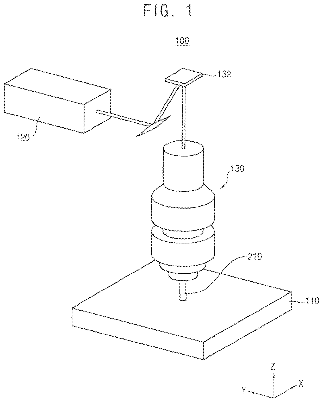
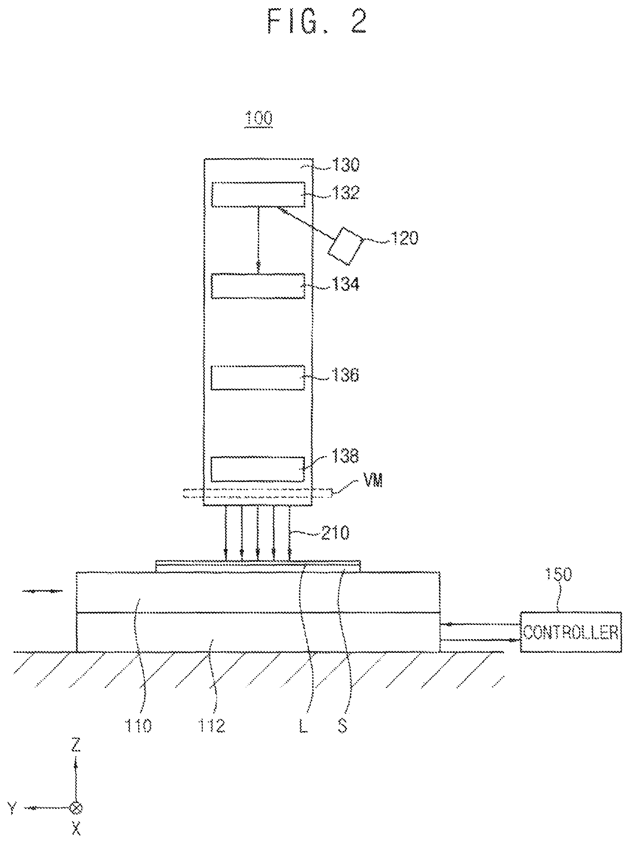
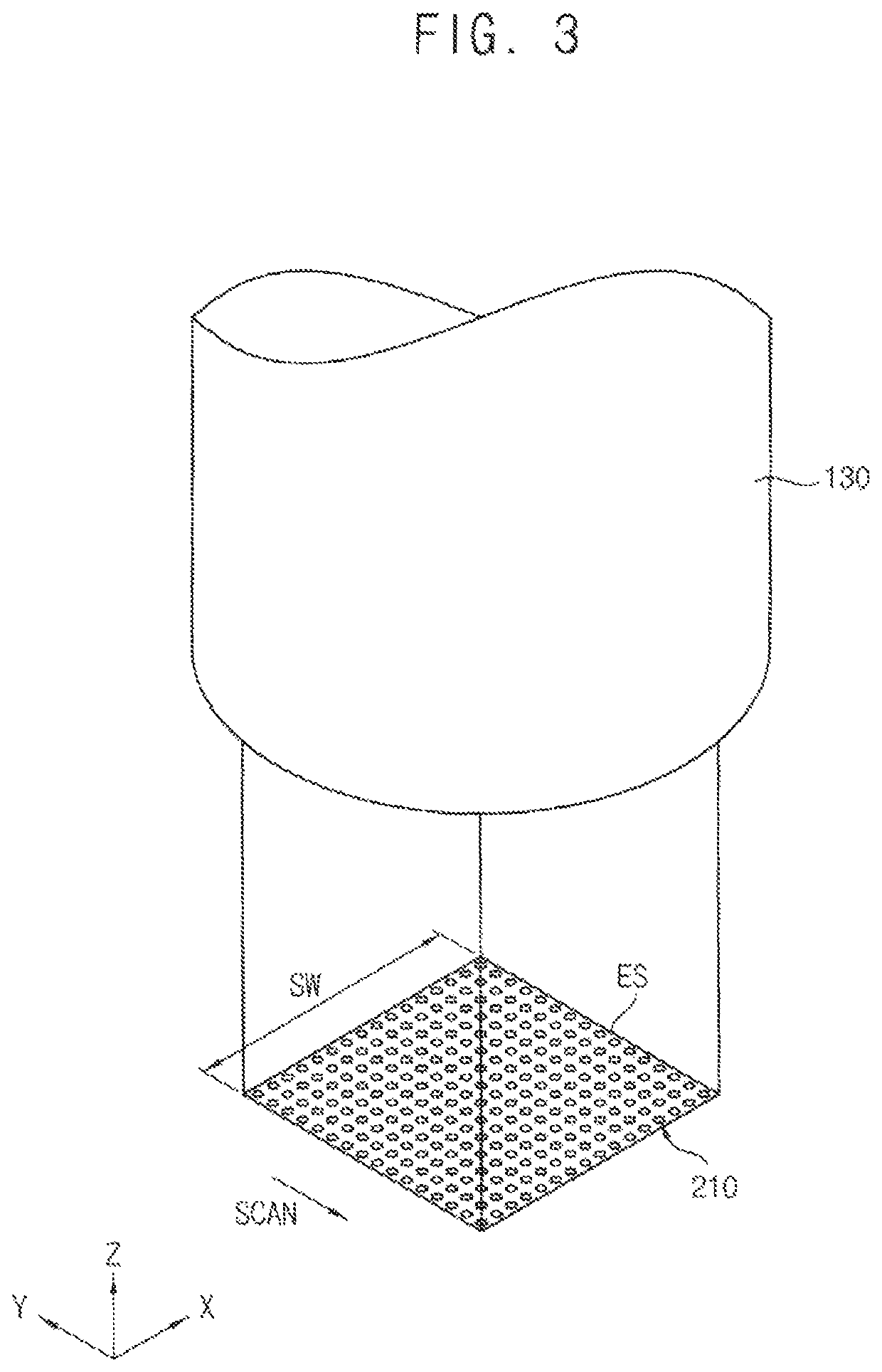
[0032]Exemplary embodiments of the present invention will be described more fully hereinafter with reference to the accompanying drawings. Like reference numerals may refer to like elements throughout the accompanying drawings.

[0033]It will be understood that the terms “first,”“second,”“third,” etc. are used herein to distinguish one element from another, and the elements are not limited by these terms. Thus, a “first” element in an exemplary embodiment may be described as a “second” element in another exemplary embodiment.

[0034]Herein, when two or more elements or values are described as being substantially the same as or about equal to each other, it is to be understood that the elements or values are identical to each other, indistinguishable from each other, or distinguishable from each other but functionally the same as each other as would be understood by a person having ordinary skill in the art.

[0035]It will be further understood that when two components or directions are de...


PUM

PropertyMeasurementUnit
heightaaaaaaaaaa
thicknessaaaaaaaaaa
radius of curvatureaaaaaaaaaa

Abstract

A maskless exposure method includes spatially modulating a light output from a light source into a pattern beam having a mask pattern, condensing the modulated pattern beam into a first group of spot beams having a first focal position on a Z-axis substantially perpendicular to an exposure surface of an object layer, and into a second group of spot beams having a second focal position different from the first focal position, and scanning the object layer with the first and second groups of spot beams. The object layer has a first height and a second height different from the first height.

Description

CROSS-REFERENCE TO RELATED APPLICATIONS[0001]This application claims priority under 35 U.S.C. § 119 to Korean Patent Application No. 10-2017-0151818, filed on Nov. 14, 2017, the disclosure of which is incorporated by reference herein in its entirety.TECHNICAL FIELD[0002]Exemplary embodiments of the present invention relate to a maskless exposure method, a maskless exposure apparatus, and a method of manufacturing a semiconductor device using the same. More particularly, exemplary embodiments relate to a maskless exposure method using a spatial light modulator, a maskless exposure apparatus, and a method of manufacturing a semiconductor device using the same.DISCUSSION OF THE RELATED ART[0003]An exposure apparatus may be used to form a pattern on a substrate such as, for example, a flat panel display (FPD) or a semiconductor wafer. As the size of the substrate increases and the pattern to be formed requires increased precision, manufacturing costs of a photomask increase. A maskless ...

Claims


Application Information

Patent Timeline
Patent Type & Authority Patents(United States)
IPC IPC(8): G03F7/20H01L21/027
CPCG03F7/703G03F7/2059G03F7/2051H01L21/0274G03F7/70291G03F7/2002G03F7/70275G03F7/70641G03F7/70116H01L21/0273
Inventor LEE, SANG-MINPARK, SANG-HYUNJOO, WON-DON
Owner SAMSUNG ELECTRONICS CO LTD
Why Eureka
Try Eureka