Manufacturing method of connector structure

a manufacturing method and connector technology, applied in the direction of elastomeric connecting elements, fixed connections, printed circuit aspects, etc., can solve the problems of difficult to reduce the manufacturing cost of typical connector structures, difficult to transmit high-frequency signals, etc., and achieve the effect of low manufacturing costs and advantageous high-frequency signal transmission

Active Publication Date: 2020-06-02
UNIMICRON TECH CORP
View PDF9 Cites 0 Cited by
  • Summary
  • Abstract
  • Description
  • Claims
  • Application Information

AI Technical Summary

Benefits of technology

[0005]The disclosure is related to a manufacturing method of a connector structure, which has low manufacturing cost and is advantageous for high-frequency signal transmission.
[0012]Based on the above, the manufacturing method of the connector structure of the disclosure is performed by forming the conductive via at a position where the conductive elastic cantilever is jointed to the dielectric layer to avoid that unnecessary metal layer is formed on the dielectric layer, thereby reducing the manufacturing cost. On the other hand, on basis that there is no conductive via or metal layer in the orthogonal projection range of the free end of the conductive elastic cantilever on the dielectric layer, the capacitance effect in the connector structure is significantly reduced, which is advantageous for high-frequency signal transmission.

Problems solved by technology

Being limited by manufacturing process, a metal layer is formed adjacent to the conductive via and not removable.
First of all, based on the relative positions of the two terminals and the conductive via as well as the metal layer, the capacitance effect generated in typical connector structure is not likely to be reduced and thus making it difficult to transmit high-frequency signal.
Moreover, it is difficult to reduce the manufacturing cost of typical connector structure due to formation of metal layer.

Method used


Image

  • Manufacturing method of connector structure
  • Manufacturing method of connector structure
  • Manufacturing method of connector structure

Examples


Embodiment Construction

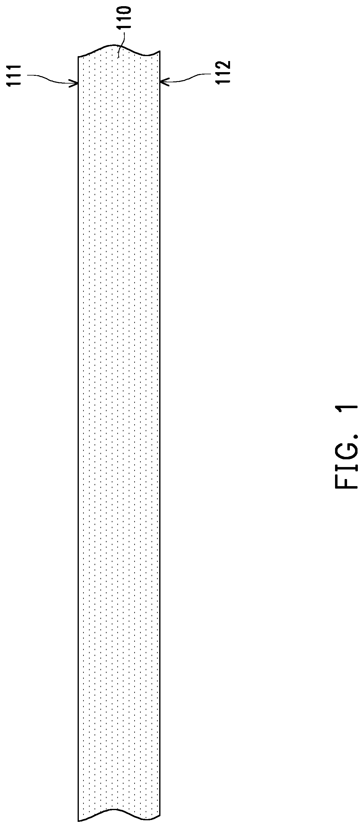
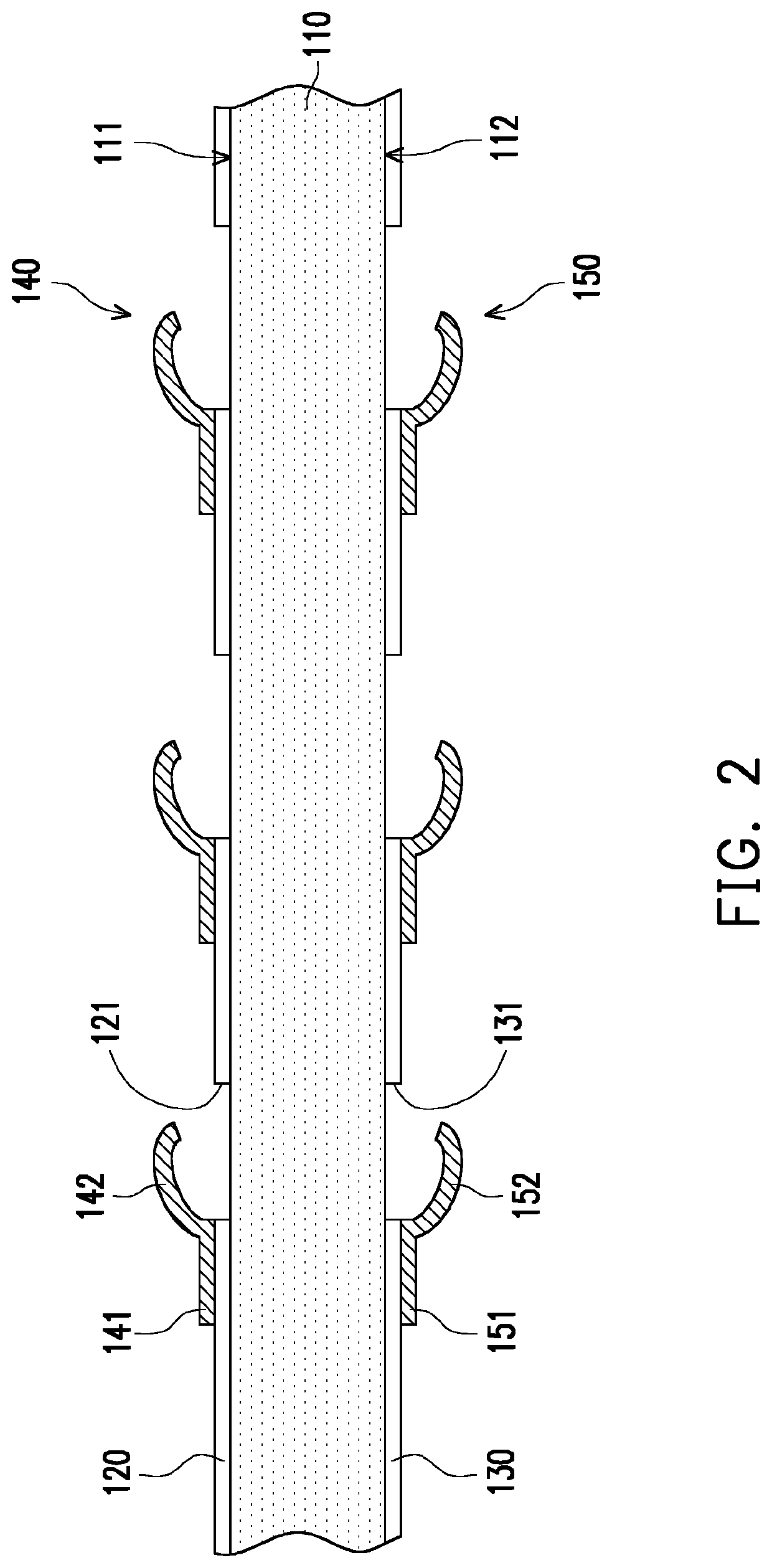
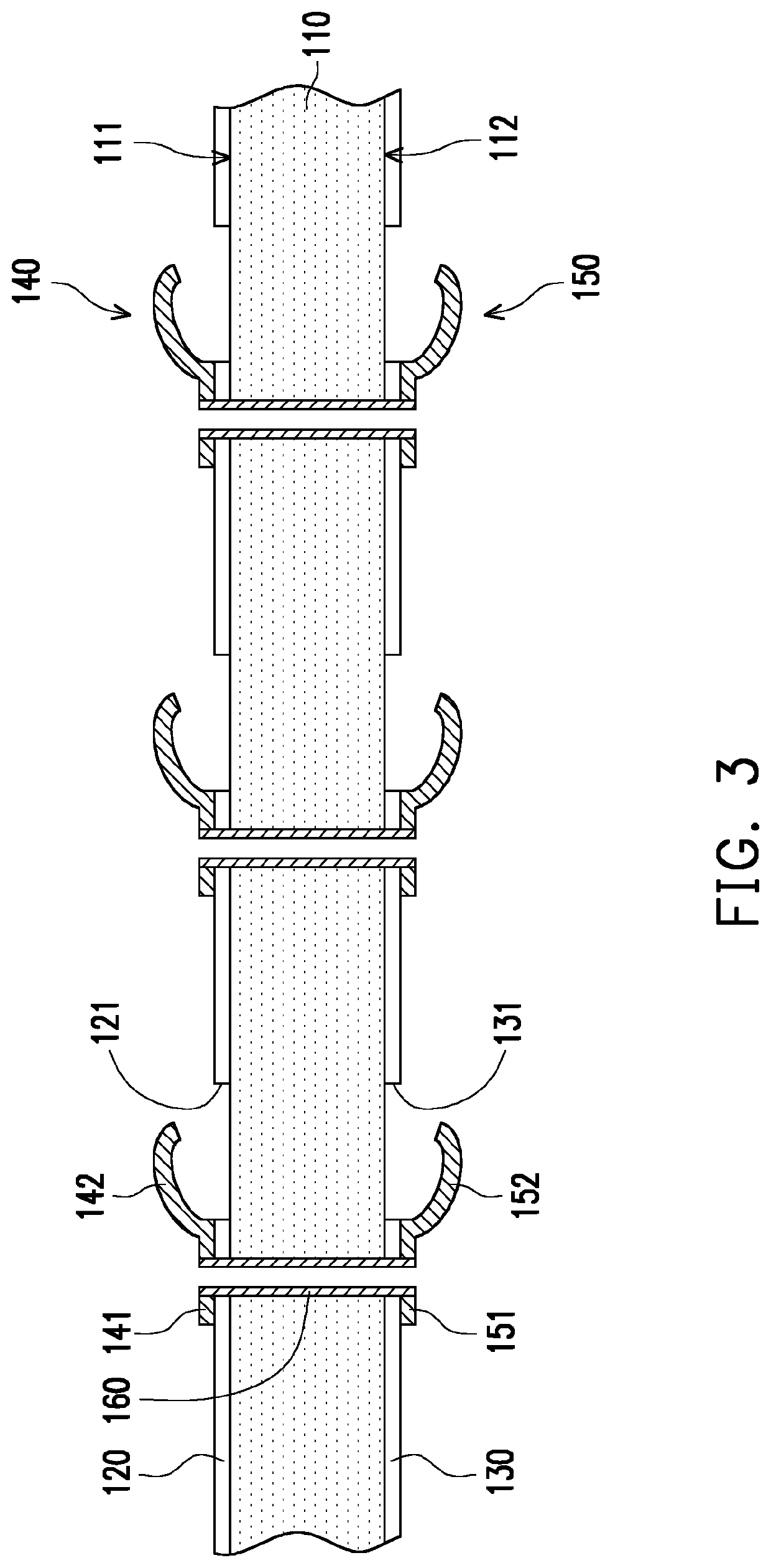
[0017]FIG. 1 to FIG. 4 are schematic flowcharts of a manufacturing process of a connector structure according to an embodiment of the disclosure. Referring to FIG. 1, in the embodiment, a dielectric layer 110 is provided, which may be formed of polyimide (PI) or polyethylene terephthalate (PET), the disclosure is not limited thereto. Specifically, the dielectric layer 110 has a first surface 111 and a second surface 112 opposite to each other, and the first surface 111 and the second surface 112 are parallel with each other, for example. Next, referring to FIG. 2, a first adhesive layer 120 is formed on the first surface 111, and a second adhesive layer 130 is formed on the second surface 112.

[0018]In an embodiment, the first adhesive layer 120 may be completely formed on the first surface 111; then a portion of the first adhesive layer 120 is removed to form at least one first opening 121 (a plurality of first openings are shown for exemplary purpose) such that a portion of the fir...


PUM

PropertyMeasurementUnit
conductiveaaaaaaaaaa
frequencyaaaaaaaaaa
dielectricaaaaaaaaaa

Abstract

A manufacturing method of connector structure including the following steps is provided. First, providing a dielectric layer having. Then, forming a first adhesive layer and a second adhesive layer on two opposite sides of the dielectric layer respectively. Then, providing at least one first conductive elastic cantilever and at least one second conductive elastic cantilever, wherein the first conductive elastic cantilever comprises a first fixing end portion and a first free end portion, and the second conductive elastic cantilever comprises a second fixing end portion and a second free end portion. Then, fixing the first fixing end portion and the second fixing end portion to the first adhesive layer and the second adhesive layer respectively, wherein the first fixing end portion is aligned with the second fixing end portion. Afterward, forming at least one conductive via for electrically connecting the first conductive elastic cantilever with the second conductive elastic cantilever.

Description

CROSS-REFERENCE TO RELATED APPLICATION[0001]This application claims the priority benefit of China application serial no. 201810677328.5, filed on Jun. 27, 2018. The entirety of the above-mentioned patent application is hereby incorporated by reference herein and made a part of this specification.BACKGROUNDTechnical Field[0002]The disclosure is related to a connector structure, and particularly to a manufacturing method of a connector structure.Description of Related Art[0003]In recent years, along with advancement of technical industries, electronic products such as notebook computer, tablet PC and smart phone are frequently used in our daily life. The form and function of electronic products are varied; therefore, a circuit board applied to electronic products plays an important role in related techniques. In order to increase application of circuit board, different types of connectors may be disposed on the circuit board so that the circuit board can be connected with other electr...

Claims


Application Information

Patent Timeline
Patent Type & Authority Patents(United States)
IPC IPC(8): H01R43/00H01R12/55
CPCH01R43/007H01R12/55H01R43/20H01R12/526H05K1/113H05K2201/10265
Inventor CHUANG, YU-HSIANGLI, GUODONGLEI, HEZHANG, JIANYU
Owner UNIMICRON TECH CORP
Why Eureka
Try Eureka