Method and device for plasma treatment of substrates

a substrate and plasma treatment technology, applied in the direction of electrical equipment, semiconductor/solid-state device manufacturing, electric discharge tubes, etc., can solve the problems of sagging substrates, poor heat contact, further impede coupling, etc., and achieve the effect of time-consuming adjustment of loading pins and small amount of time spen

Active Publication Date: 2020-07-07
EV GRP E THALLNER GMBH
View PDF29 Cites 0 Cited by
  • Summary
  • Abstract
  • Description
  • Claims
  • Application Information

AI Technical Summary

Benefits of technology

[0018]In addition, the time-consuming adjustment of the loading pins is eliminated, which in the outer electrode unit is replaced by the mechanical construction of the inner electrode unit and leads to a smaller amount of time spent in comparison to the conventional designs.
[0019]Another advantage comes from the large-area seating in the handling of thin substrates, which cannot be handled with the loading pin design because of their bending. The size of the inner electrode unit is adaptable and thus suitable for different types of substrates.

Problems solved by technology

The coupling is done via a dielectric electrode, which has the disadvantage that a metal coating of this electrode can further impede the coupling.
Mechanical clamping devices such as, for example, 3-point mountings, are used, hut cause sagging substrates, abrasion, and poor heat contact.
A disadvantage is that thin wafers bend greatly, and thus an inaccurate positioning of the substrate on the pins also results.
Structures with loading pins as sample pickup devices have the following problem: because of the loading pin, there is inhomogeneity of the plasma field, which leads to voltage peaks during the process at the necessary recesses.

Method used


Image

  • Method and device for plasma treatment of substrates
  • Method and device for plasma treatment of substrates
  • Method and device for plasma treatment of substrates

Examples


Embodiment Construction

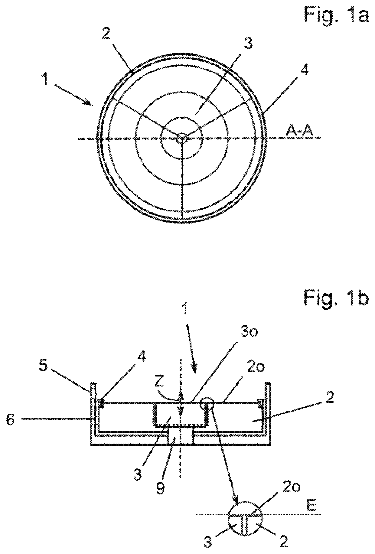
[0052]FIG. 1a shows a top view of an in particular lower, first electrode 1 in a plasma chamber 6, in particular with an integrated substrate holding device according to an embodiment of the invention. The holding of a substrate 7 is done in particular by vacuum strips and / or by a focus ring 4, 4′. The first electrode 1 has an outer electrode unit 2 that is designed as a ring electrode and an inner electrode unit 3. The inner electrode unit 3 is laterally limited and enclosed by the outer electrode unit 2. The substrate 7 is held on the outside by the focus ring 4, 4′ that surrounds, in particular encloses, the substrate 7.

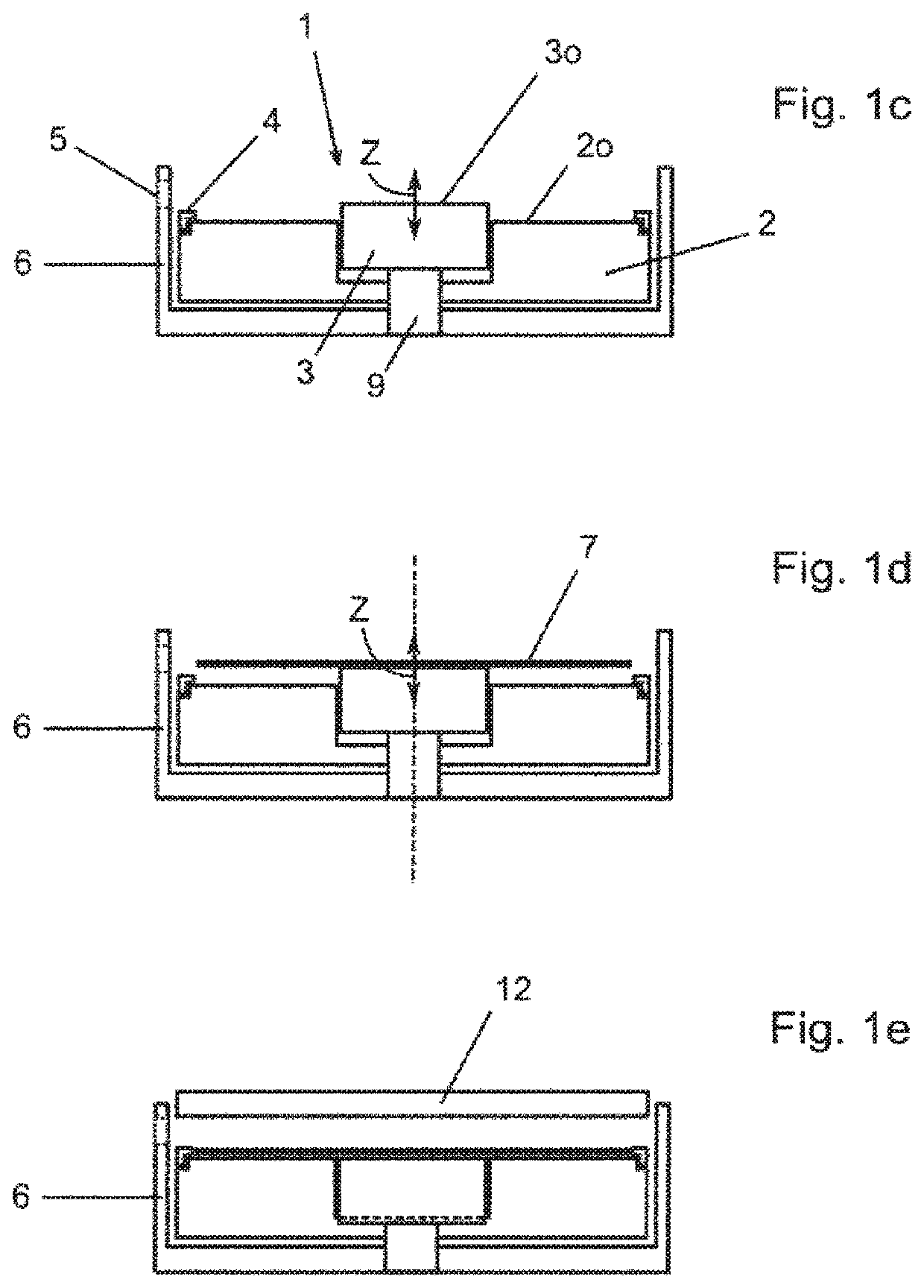
[0053]FIG. 1b shows a cross-section through the first electrode 1 and the plasma chamber 6. The first electrode 1 that is formed in two parts or from the inner electrode unit 3 and the outer electrode unit 2 is used as a holding device for the substrate 7, in particular with a flat surface 2o of the outer electrode unit 2. The inner electrode unit 3 is used to loa...


PUM

PropertyMeasurementUnit
diametersaaaaaaaaaa
diametersaaaaaaaaaa
diametersaaaaaaaaaa

Abstract

A device for bombarding at least one substrate with a plasma with a first electrode and a second electrode that can be arranged opposite thereto, which electrodes are formed together producing the plasma between the electrodes wherein at least one of the electrodes is formed from at least two electrode units. In addition, this invention relates to a corresponding method.

Description

FIELD OF THE INVENTION[0001]The present invention relates to a device for bombarding a substrate with a plasma as well as a corresponding method for bombarding a substrate with a plasma.BACKGROUND OF THE INVENTION[0002]Many semiconductor production processes contain one or more plasma treatment steps. The plasma can be used, e.g., for coating a substrate, for depositing semiconductor layers, for etching a substrate, for plasma activation, or for creating an ion reservoir. In this case, gases such as, e.g., silane (SiH4), helium (He), argon (Ar), hydrogen (H2) and / or nitrogen trifluoride (NF3) are directed into the plasma chamber. SiH4 or H2 are used, e.g., in the deposition of semiconductor lavers, and NF3 is used in the plasma etching of semiconductor layers. If a mixture made of noble gas and a reactive gas is used, the layer composition can be controlled by the adjustment of the gas mixture ratios. Thus, not only metals, but also oxides, nitrides and carbides can be deposited. Wo...

Claims


Application Information

Patent Timeline
Patent Type & Authority Patents(United States)
IPC IPC(8): H01L21/00H01J37/32H01L21/687H01L21/3065H01L21/67
CPCH01J37/32091H01J37/32532H01J37/32733H01L21/68785H01J37/32568H01J37/32715H01L21/3065H01L21/67069
Inventor GLINSNER, THOMASFLOTGEN, CHRISTOPHBERNAUER, JOHANNWAGENLEITNER, THOMASWIESER, THOMASSCHMID, FLORIANPLACH, THOMASANZENGRUBER, ROMANNONES, ALEXANDERKRIEBISCH, UWE
Owner EV GRP E THALLNER GMBH
Why Eureka
Try Eureka