Method of manufacturing a smartcard

a smartcard and manufacturing method technology, applied in the field of smartcards, can solve the problems of not allowing traditional soldering, damage to polyurethane (pu), and damage to the structure of the smartcard, and achieve the effect of high durability

Active Publication Date: 2020-07-28
ZWIPE
View PDF12 Cites 0 Cited by
  • Summary
  • Abstract
  • Description
  • Claims
  • Application Information

AI Technical Summary

Benefits of technology

[0016]Preferably the melting temperature of the material forming the extension members is at least 10° C. above the melting temperature of the material forming the card body. This permits a clear range in which the card body can be thermally laminated, i.e. by melting and combining layers of material to form the card body around the circuit, without damaging the extension members. Preferably, the material forming the extension members has a melting temperature above 200° C., and preferably above 210° C.
[0017]The extension members may be formed from any suitable material, but are preferably formed from a metallic material. The use of a metallic material allows for the card to employ a metal-to-metal connection between the contact pad and the flexible circuit, which provides high durability to provide maximum life to the smartcard—a typical payment card, for example, must have a minimum lifetime of three years.

Problems solved by technology

In order to ensure sufficient longevity of the card, it is necessary to be aware of the temperature sensitivity of the materials used typically for smartcards, which do not allow for traditional soldering.
Polyurethane (PU), which is also commonly used as filler for laminated cards, would also be damaged by exposure to temperatures in the region of 240° C.

Method used


Image

  • Method of manufacturing a smartcard
  • Method of manufacturing a smartcard

Examples


Embodiment Construction

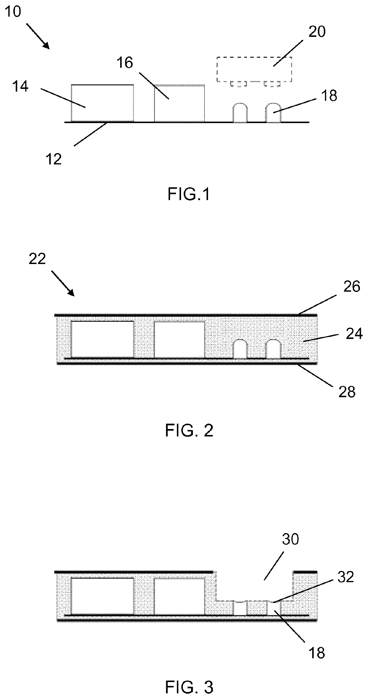
[0051]FIG. 1 illustrates a flexible printed circuit board assembly (FPCBA) 10 for a smartcard. The circuit board assembly 10 comprises a flexible printed circuit board 12 on which are mounted various components to be embedded within the smartcard. These components should each be capable of withstanding the temperatures and pressures arising during a thermal lamination process, such as that described later.

[0052]Illustrated in FIG. 1 are a secure element 14 and a fingerprint processing unit 16, which are both connected to the flexible circuit board 12. However, in various embodiments, one or other of these may not be present, and / or further components may also be present.

[0053]The fingerprint processing unit 16 will form part of a fingerprint authentication module, when connected to a fingerprint sensor 130, such as the area fingerprint reader 130 shown in FIG. 6. The processing unit 16 comprises a microprocessor that is chosen to be of very low power and very high speed, so as to be...


PUM

PropertyMeasurementUnit
heightaaaaaaaaaa
temperatureaaaaaaaaaa

Abstract

A method of manufacturing a smartcard may include providing a flexible smartcard circuit, forming conductive extension members on and extend away from the flexible circuit from a high melting point solder material, and laminating the flexible circuit to form a smartcard body. A cavity is then milled in the smartcard body to expose the ends of the extension members, and a contact pad is inserted into the cavity and electrically connected to extension members using a low melting temperature tin-bismuth solder using ultrasonically soldering, so as to avoid heat damage to the card body.

Description

TECHNICAL FIELD[0001]The present invention relates to a smartcard and to its method of manufacture, and more particularly to the manner in which a component to be exposed from the smartcard is mounted to an embedded circuit board of the smartcard during manufacture.BACKGROUND OF THE INVENTION[0002]The term smartcard refers generally to any pocket-sized card that has one or more integrated circuits embedded therein. Examples of common smartcard applications include payment cards, access cards, and the like.[0003]The contact pad is the designated surface area of the smartcard that permits electrical contact to be made with an external device. Where the smartcard contains sensitive data, such as in the case of payment cards and the like, a secure element is used to store the data. A secure element is a tamper-proof chip that provides a secure memory and execution environment in which application code and application data can be securely stored and administered. The secure element ensur...

Claims


Application Information

Patent Timeline
Patent Type & Authority Patents(United States)
IPC IPC(8): G06K19/077B32B37/12G06K19/07H05K1/18
CPCG06K19/07722G06K19/07769B32B37/1284G06K19/07749G06K19/0718G06K19/07747G06K19/07754G06K19/0773H05K1/182B42D25/40G06K19/07745
Inventor SNELL, DEVINLAVIN, JOSE IGNACIO WINTERGERST
Owner ZWIPE
Why Eureka
Try Eureka