Interconnect bump structures for photo detectors

a bump structure and photo detector technology, applied in the field of interconnections, can solve the problems of limiting the size of the manufacturer to make the large format fpa pixel pitch, difficult alignment, etc., and achieve the effect of reducing the wettability of bump materials and avoiding high press pressure for hybridization

Active Publication Date: 2020-07-28
SENSORS UNLTD
View PDF8 Cites 2 Cited by
  • Summary
  • Abstract
  • Description
  • Claims
  • Application Information

AI Technical Summary

Benefits of technology

[0006]Each bump can electrically connect one pixel of the PDA to the ROIC. The PDA can have a pixel pitch size of 10 μm or less. Pixels of the PDA can be isolated from one another by mesa trenches with sidewall passivation. The mesa trenches can be etched into the PDA to provide relief of the stresses which otherwise lead to misalignment through wafer bowing and also to provide electrical isolation between pixels. Misalignment caused by die bowing can be compensated by interconnecting deep-trench PDA pixels with stress and bowing released due to the deep trench etch with soft ROIC bumps through intermetallic bonding.
[0007]Mesas between the mesa trenches on the PDA can mate with ROIC bumps less than 1 um deep through intermetallic bonding, wherein high-pressure pressing of excess indium materials on each side of PDA and ROIC can be avoided due to the much smaller ROIC bumps mating directly to PDA contacts through intermetallic bonding, and wherein short circuits between neighboring pixels can be eliminated with this interconnection structure due to a high pressure press-free bonding process. Stress due to the coefficient of thermal expansion mismatch between the PDA and the ROIC can be reduced due to high aspect ratio (height:diameter) with this interconnect structure.
[0009]Depositing bumps on the ROIC can include using evaporation to deposit the bumps, wherein the bumps include indium. Depositing the bumps on the ROIC can include keeping the bumps under a dimension of 1 μm in a direction from the ROIC to the PDA. The bump height is adjustable to fulfill the requirement of suppressing the bowing of die, a factor which is also reduced by the stress relief during the mesa isolation etch. Assembling the PDA and ROIC together can include plasma treatment followed by reflow of the PDA and / or ROIC to achieve intermetallic bonding between the ROIC, the contacts, and the bumps, e.g., so that the traditional high press pressure for hybridization is avoided.
[0010]The method can include plasma treating the PDA and ROIC to remove local oxidation on contacts of the PDA and ROIC. Plasma treating the PDA and ROIC can include adjusting the surface polarity of a dielectric outer surface sub-layer of a sidewall passivation layer of the PDA and ROIC to reduce wettability of bump material to the dielectric sub-layer.

Problems solved by technology

Traditional techniques use bumps with height to diameter ratios that make alignment difficult when interconnecting components.
As a result, lateral expansion and the alignment difficulties limit how small a manufacturer can make the large format FPA pixel pitch.

Method used


Image

  • Interconnect bump structures for photo detectors
  • Interconnect bump structures for photo detectors

Examples


Embodiment Construction

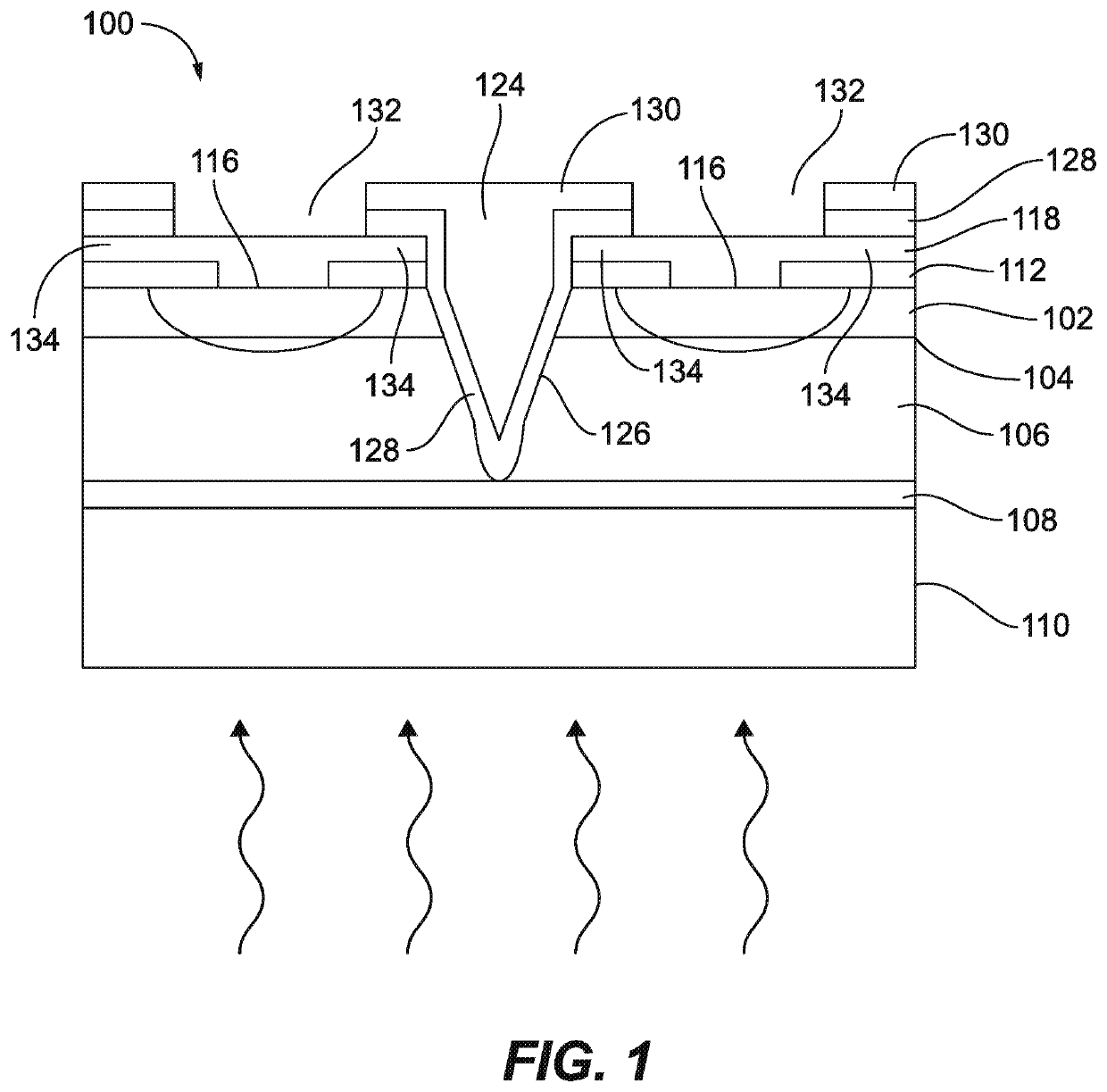
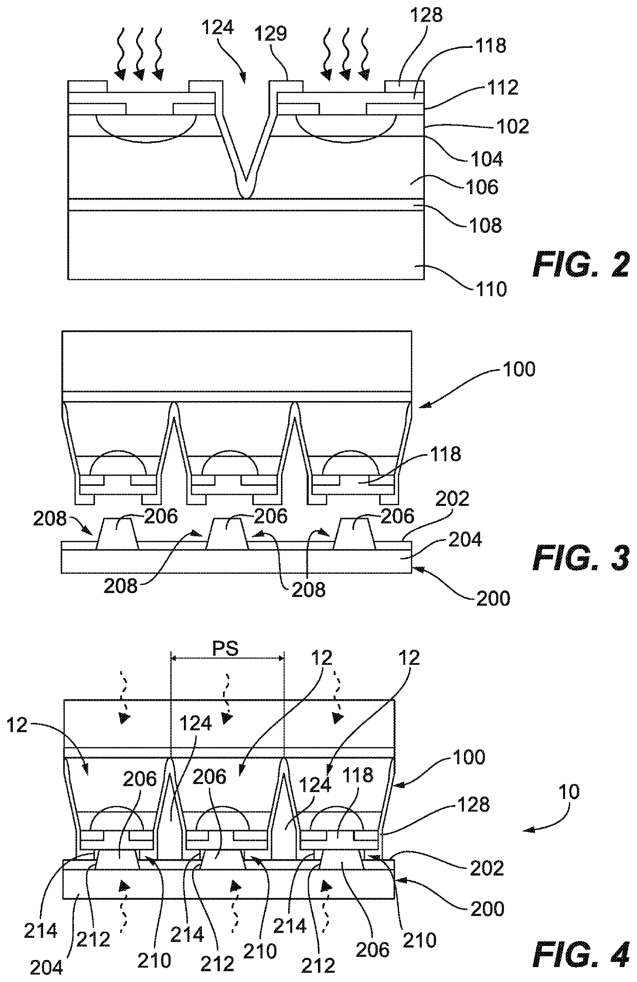
[0018]Reference will now be made to the drawings wherein like reference numerals identify similar structural features or aspects of the subject disclosure. For purposes of explanation and illustration, and not limitation, a partial view of an exemplary embodiment of a photodiode array (PDA) in accordance with the disclosure is shown in FIG. 1 and is designated generally by reference character 100. Other embodiments of PDAs in accordance with the disclosure, or aspects thereof, are provided in FIGS. 2-4, as will be described. The systems and methods described herein can be used to facilitate assembly of PDAs with read out integrated circuits (ROICs) and to reduce pixel pitch size relative to traditional configurations.

[0019]The photodiode array 100 includes an absorption layer 106, a cap layer 102 disposed on the surface 104 of the absorption layer 106, and a plurality of pixel diffusion areas 116 within the cap layer 102. The absorption layer 106 can be disposed on a buffer layer 10...


PUM

PropertyMeasurementUnit
sizeaaaaaaaaaa
pitch sizeaaaaaaaaaa
heightaaaaaaaaaa

Abstract

A method of assembling a photodetector assembly includes depositing bumps on a read out integrated circuit (ROIC) without depositing bumps on a photodiode array (PDA). The method includes assembling the PDA and ROIC together wherein each bump electrically interconnects the ROIC with a respective contact of the PDA. A photodetector assembly includes a PDA. A ROIC is assembled to the PDA, wherein the ROIC is electrically interconnected with the PDA through a plurality of electrically conductive bumps. Each bump is confined within a respective pocket between the ROIC and a respective contact of the PDA. The disclosed methods can enable focal plane array manufacturers to achieve low-cost production of ultra-fine pitch, large format imaging arrays.

Description

BACKGROUND OF THE INVENTION1. Field of the Invention[0001]The present disclosure relates to interconnections, and more particularly to bump structures for electrically interconnecting components such as in interconnecting photodetector array components.2. Description of Related Art[0002]Fine pitch, large format focal plane arrays (FPAs), require small interconnect bumps and minimum lateral expansion after hybridization. Traditional techniques use bumps with height to diameter ratios that make alignment difficult when interconnecting components. As a result, lateral expansion and the alignment difficulties limit how small a manufacturer can make the large format FPA pixel pitch.[0003]The conventional techniques have been considered satisfactory for their intended purpose. However, there is an ever present need for improved bump structures for interconnecting components like focal plane arrays. This disclosure provides a solution for this problem.SUMMARY OF THE INVENTION[0004]A photod...

Claims


Application Information

Patent Timeline
Patent Type & Authority Patents(United States)
IPC IPC(8): H01L27/146H01L25/16H01L23/488H01L23/00
CPCH01L27/14636H01L24/11H01L24/16H01L24/81H01L25/167H01L27/1463H01L27/1469H01L27/14634H01L27/14643H01L2224/10145H01L2224/1145H01L2224/13109H01L2224/16014H01L2224/8181H01L2224/81913H01L2924/3511
Inventor ZHANG, WEIMALCHOW, DOUGLAS STEWARTEVANS, MICHAEL J.HUANG, WEIBEREZNYCKY, PAUL L.PAIK, NAMWOONG
Owner SENSORS UNLTD
Why Eureka
Try Eureka