Dynamic high-speed high-sensitivity imaging device and imaging method

a high-sensitivity imaging and high-speed technology, applied in the field of dynamic high-speed high-sensitivity imaging technology, can solve the problems of limited imaging speed, high cost and large size of imaging devices, and limitations of imaging speed in imaging devices configured for single-pixel detection, etc., to achieve the effect of exceeding the speed limit of continuous imaging technology, high signal-to-noise ratio, and cost reduction

Active Publication Date: 2020-09-01
THE UNIV OF TOKYO +1
View PDF27 Cites 6 Cited by
  • Summary
  • Abstract
  • Description
  • Claims
  • Application Information

AI Technical Summary

Benefits of technology

[0037]According to the present invention, a high-speed imaging device which can fully utilize a band (a signal detection limit speed) of a single or non-array type high-speed / high-sensitivity detectors in the world for the first time (if a capacity is GHz or less, 109 sheets (lines) / second) and greatly exceeds the speed limit of continuous imaging technology in the related art can be provided.
[0038]According to the present invention, general-purpose and various types of high-sensitivity imaging including visible fluorescence imaging which was impossible in imaging methods using a single pixel detector in the related art can be performed using a universal optical system. Also, according to the present invention, since a simple optical system can be adopted, hardly any optical signal is lost and hardly any noise is introduced. Thus, imaging with a high signal-to-noise (S / N) ratio can be performed.
[0039]According to the present invention, since an optical system and an electrical system which are used are simple, costs can be greatly decreased and compactness can be achieved as compared with all imaging techniques in the related art.

Problems solved by technology

In an imaging device using array type detecting elements, there are limitations on an imaging speed thereof from electrical restrictions when the elements are operated and a problem in that the imaging device is expensive and large in size.
For this reason, mechanical / electrical constraints involved in spatiotemporally changing illumination light occur and there are limitations on an imaging speed in the imaging device configured for single pixel detection.
For example, there are limitations on a speed of mechanically performing spatial-scanning with a laser in a confocal microscope and an image cannot be captured at high speed.
In such a method, since a speed of radiating lighting serves as a constraint, imaging is slow.
Furthermore, an imaging device using STEAM is very expensive and large in size, an applicable light wavelength range is limited to long wavelengths, and thus it is difficult to achieve high sensitivity in a visible light range.
For this reason, there is a problem in that STEAM cannot be applied to a visible fluorescence wavelength region necessary for application to the fields of life sciences / medicine.

Method used


Image

  • Dynamic high-speed high-sensitivity imaging device and imaging method
  • Dynamic high-speed high-sensitivity imaging device and imaging method
  • Dynamic high-speed high-sensitivity imaging device and imaging method

Examples


example 1

[0100]Next, the present invention will be described in detail using examples.

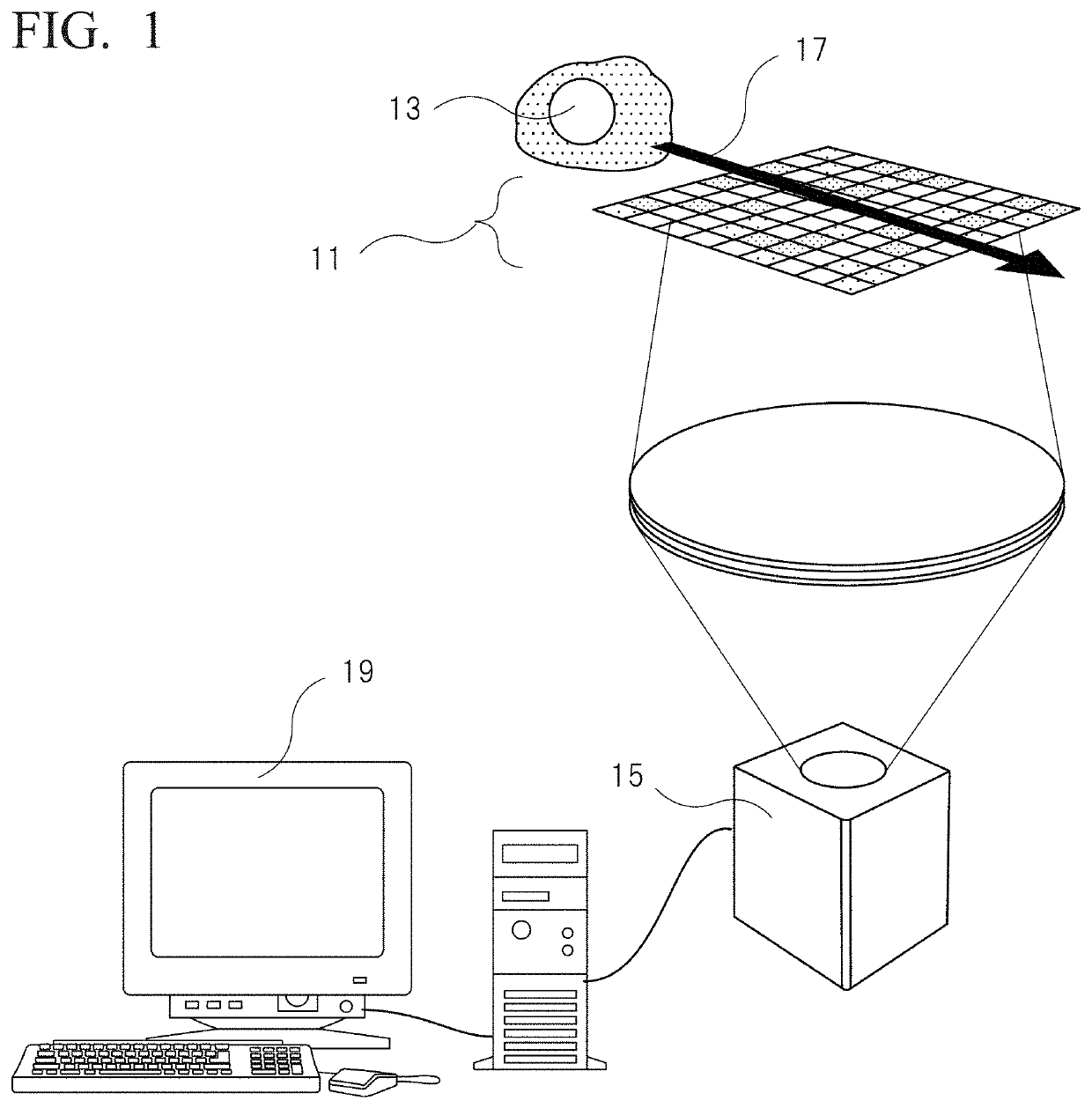
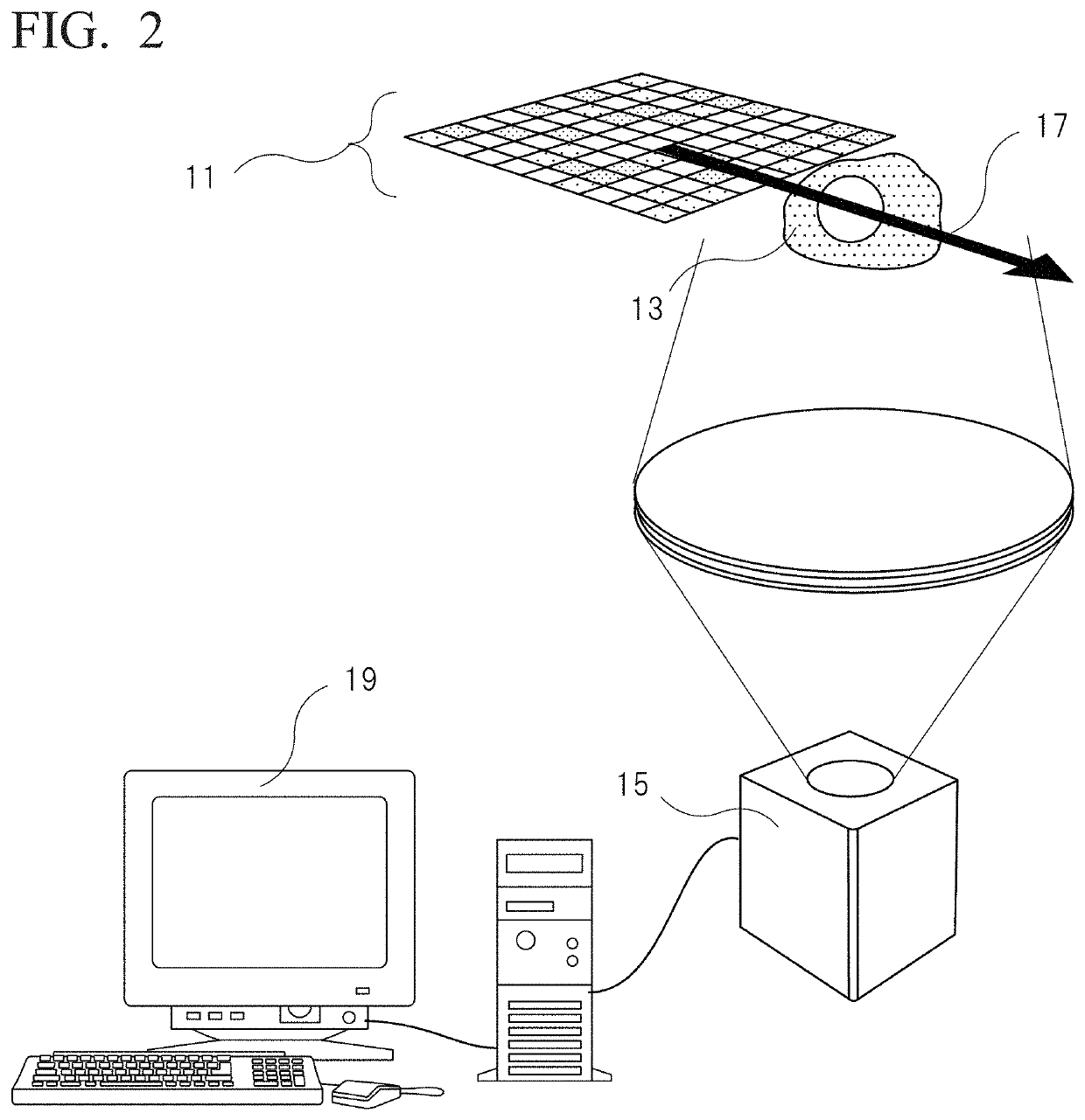
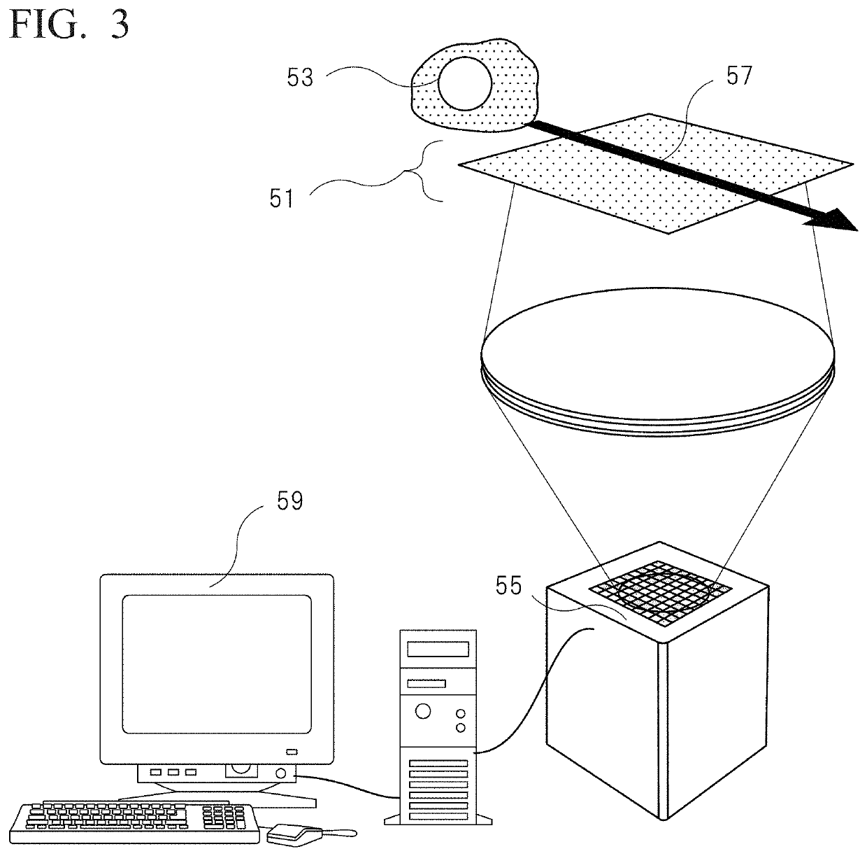
[0101]FIG. 16 is a schematic diagram of a device in Example 1. The device relates to a device in which the object to be observed moves, an irradiation pattern through which light is radiated to the object to be observed is obtained using a light source and a mirror, and light transmitted through the object to be observed is observed so that an image of the object to be observed is reproduced.

[0102]An M470L3-C1 / blue (a wavelength of 47 nm) Olympus BX & Collimator for IX LED (1000 mA) manufactured by Thorlabs, Inc. was used as a light source. Note that, unlike a case in which coherent light such as a laser is used, in the case in which non-coherent light such as a light emitting diode (LED) and a lamp was used, spots were not observed. Thus, accuracy was improved. In addition, a case in which continuous light was used was more appropriate for high speed imaging than a case in which pulsed light was used.

[0103...

example 2

[0110]Next, multicolor imaging will be described. The multicolor imaging is technology in which an object to be observed stained in multiple colors using a plurality of cell fluorescent labels is observed using a combination of a plurality of optical elements so that a color image is reconstructed. Note that the object to be observed is not limited to cells. Furthermore, light to be observed is not limited to fluorescence. A technique of dying an object to be observed is not limited to a cell fluorescent label and may use dyes or the like. The object to be observed through the multicolor imaging is not limited to a stained object to be observed and may be a colored object to be observed.

[0111]Multi-color imaging of cells of which cell nuclei, cytoplasm, cell membranes, or the like are stained in multiple colors, which has been performed in fluorescence activated cell sorting (FACS) in the related art, can be performed using a combination in which a plurality of cell fluorescent labe...


PUM

PropertyMeasurementUnit
wavelengthaaaaaaaaaa
timeaaaaaaaaaa
optical characteristicsaaaaaaaaaa

Abstract

Any one or both of an optical system with a structured lighting pattern and a structured detecting system having a plurality of regions with different optical characteristics are used. In addition, optical signals from an object to be observed through one or a small number of pixel detectors are detected while changing relative positions between the object to be observed and any one of the optical system and the detecting system, time series signal information of the optical signals are obtained, and an image associated with an object to be observed from the time series signal information is reconstructed.

Description

CROSS REFERENCE TO RELATED APPLICATIONS[0001]This application is a 35 USC § 371 United States national stage application of International Application No. PCT / JP2016 / 055412, filed Feb. 24, 2016, which claims priority to Japanese Application No. 2015-033520, filed Feb. 24, 2015, the contents of which are incorporated herein by reference.TECHNICAL FIELD[0002]The present invention relates to dynamic high-speed high-sensitivity imaging technology in which an object to be observed and a detecting system having an optical system or a structure configured to project structured lighting are relatively displaced.[0003]Priority is claimed on Japanese Patent Application No. 2015-033520, filed Feb. 24, 2015, the content of which is incorporated herein by reference.BACKGROUND ART[0004]Japanese Unexamined Patent Application, First Publication No. 2014-175819 (Patent Literature 1) discloses an imaging system including electromagnetic wave detecting elements arranged in a two-dimensional array. In a...

Claims


Application Information

Patent Timeline
Patent Type & Authority Patents(United States)
IPC IPC(8): G01J3/00G01N21/59G01N21/53G01N21/64G01B11/00G01N21/01H03M7/30
CPCG01N21/01G01B11/00G01N21/53G01N21/6456G01N21/59H03M7/3062G01N21/64
Inventor OTA, SADAOHORISAKI, RYOICHIHASHIMOTO, KAZUKI
Owner THE UNIV OF TOKYO
Why Eureka
Try Eureka