

Heat-curable resin composition for semiconductor encapsulation and semiconductor device
a technology of heat-curable resin and semiconductor encapsulation, which is applied in the direction of semiconductor devices, semiconductor/solid-state device details, solid-state devices, etc., can solve the problems of failures significantly impairing low crosslinking density, and reduced crosslinking density, so as to improve the reliability of semiconductor devices, improve the stability of semiconductor devices, and improve the effect of heat-curable resin composition
- Summary
- Abstract
- Description
- Claims
- Application Information
AI Technical Summary
Benefits of technology
Problems solved by technology
Method used
Image

Examples
working example
[0103]The present invention is described in detail hereunder with reference to working and comparative examples. However, the invention is not limited to the following working examples.
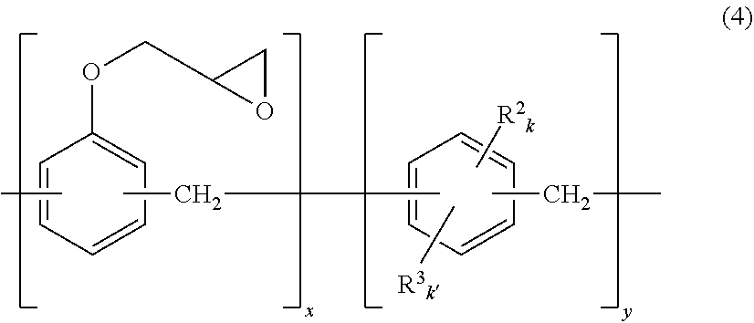
(A) Epoxy Resin
[0104](A-1) Trisphenylol methane-type epoxy resin (EPPN-501H by Nippon Kayaku Co., Ltd.; epoxy equivalent 165, softening point 54° C.)
[0105](A-2) Bisphenol A-type epoxy resin (jER-1001 by Mitsubishi Chemical Corporation; epoxy equivalent 475, softening point 64° C.)
(B) Silicone-Modified Epoxy Resin
[0106](B-1) Addition compound represented by the following formula (9) (by Shin-Etsu Chemical Co., Ltd.)
[0107]
[0108](B-2) Addition compound represented by the following formula (9) (by Shin-Etsu Chemical Co., Ltd.)
[0109]
[0110]Here, the compounds represented by the formulae (9) and (10) were produced by the above method.
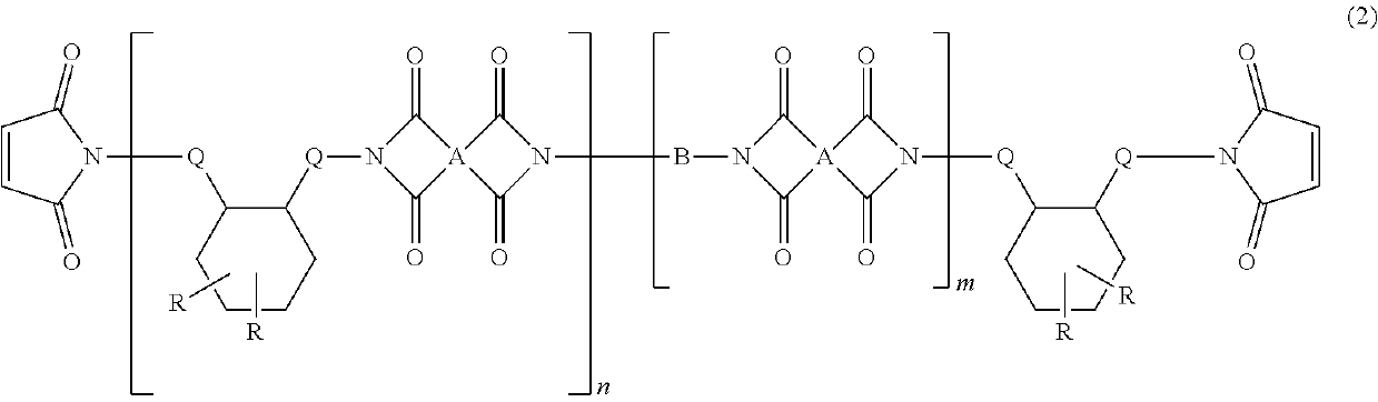
(C) Cyclic Imide Compound
[0111](C-1) Maleimide compound represented by the following formula (weight-average molecular weight 3,000; BMI-3000 by Designer Molecules Inc.)
[0112]
[0...
PUM
| Property | Measurement | Unit |
|---|---|---|
| softening point | aaaaa | aaaaa |
| melting point | aaaaa | aaaaa |
| pressure | aaaaa | aaaaa |
Abstract
Description
Claims
Application Information