Quantum dot LED structure having optically transparent layer on partially transmitting reflector for enhanced emission

a quantum dot led and partially transmitting reflector technology, applied in static indicating devices, instruments, organic semiconductor devices, etc., can solve the problems of conflicting light emission optimization is relatively costly and difficult to achieve, and the optical properties and electronic properties of layers are in conflict, so as to improve the extraction efficiency and angular light profile, enhance the on-axis light emission

Active Publication Date: 2020-11-03
SHARP KK
View PDF13 Cites 0 Cited by
  • Summary
  • Abstract
  • Description
  • Claims
  • Application Information

AI Technical Summary

Benefits of technology

[0008]The present invention provides a layer structure used for an emissive device, in particular for a quantum dot light-emitting diode (QLED) display device or an organic light-emitting diode (OLED) display device, that provides enhanced on-axis light emission. The present invention uses an additional layer or layers on top of a conventional QLED or OLED pixel, such as described in FIG. 1, to optimize extraction efficiency and angular light profile while allowing the functional layers to be selected optimally for the electronic properties of the device without additional processing of the functional layers.
[0009]In particular, embodiments of the present invention include an additional substantially transparent region and a partially reflective layer disposed on top of the functional charge transport and emissive layers. By optimizing the thickness of the substantially transparent region, the light emitted in a particular direction can be maximized because the transparent region and partially reflective layer form a cavity effect, and the direction of light emission depends on the total path length seen by an emitted light ray. The thickness of the substantially transparent region can be varied or different for each of red, green, and blue light emitting pixels so that light extraction is separately optimized for each color of light emission. Typical materials for such a transparent region, such as for example SiO2, indium tin oxide (ITO), Poly(methyl methacrylate) (PMMA), or SU-8 photoresist are robust and processed easily by standard manufacturing methods. Accordingly, simple processing of the transparent region to achieve optimal thickness can be performed while avoiding the more complex and potentially detrimental processing of the functional layers.

Problems solved by technology

A significant drawback of such a design is that each pixel must have a different thickness of electron transport layer, necessitating patterning of the functional layers.
Patterning of functional layers that act as the charge transport layers (e.g., electron or hole transport layers) constitutes a complex process that renders light emission optimization relatively costly and difficult to achieve.
As referenced above, however, patterning of functional layers that act as the charge transport layers (e.g., electron or hole transport layers) constitutes a complex process that renders light emission optimization relatively costly and difficult to achieve.
In particular, altering thicknesses of the functional layers can result in the optical properties and electronic properties of the layers being in conflict when the functional layer thickness is optimized.
Furthermore, patterning of the functional layers to give different thicknesses for different color pixels necessitates some form of masking or etching, which can detrimentally impact the electronic properties of the functional layers and increase cost and complexity of manufacture.
Conventional configurations, therefore, have not optimized light extraction and emission while maintaining other optimum device properties (e.g., electronic properties and adequate view angle control) in a manner that is efficient to manufacture.

Method used


Image

  • Quantum dot LED structure having optically transparent layer on partially transmitting reflector for enhanced emission
  • Quantum dot LED structure having optically transparent layer on partially transmitting reflector for enhanced emission
  • Quantum dot LED structure having optically transparent layer on partially transmitting reflector for enhanced emission

Examples


Embodiment Construction

[0026]Embodiments of the present invention will now be described with reference to the drawings, wherein like reference numerals are used to refer to like elements throughout. It will be understood that the figures are not necessarily to scale.

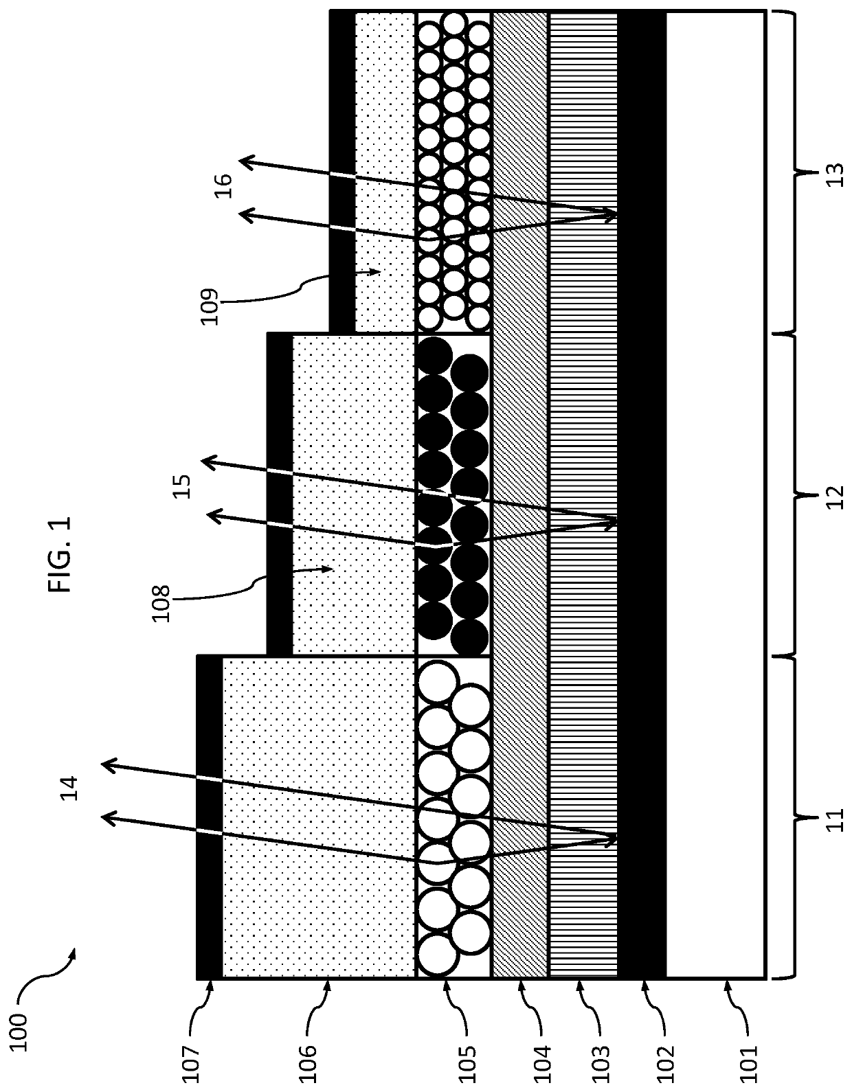
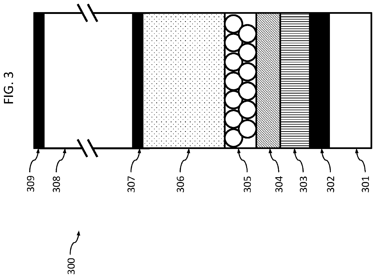
[0027]The present invention provides a layer structure used for an emissive device, in particular for a quantum dot light-emitting diode (QLED) display device or an organic light-emitting diode (OLED) display device, that provides enhanced on-axis light emission. The present invention uses an additional layer or layers on top of a conventional QLED or OLED pixel, such as described in FIG. 1, to optimize extraction efficiency and angular light profile while allowing the functional layers to be a selected optimally for the electronic properties of the device without additional processing of the functional layers.

[0028]In particular, embodiments of the present invention include an additional substantially transparent region and a partially reflec...


PUM

PropertyMeasurementUnit
thicknessaaaaaaaaaa
thicknessaaaaaaaaaa
thicknessaaaaaaaaaa

Abstract

A light-emitting device for use in a display device has enhanced directional light emission, and enhanced on-axis light emission in particular. A light-emitting device includes a layer structure that includes from a non-emitting side: a first electrode layer; a first charge transport layer; an emissive layer; a second charge transport layer; a second electrode layer; an optically transparent layer; and a partially transmitting reflector layer. The light-emitting device comprises a plurality of regions and each region emits light of a different wavelength, such as for example red, green, and blue light-emitting regions. The optically transparent layer is present in at least one of the plurality of regions. The optically transparent layer may be present in more than one of the plurality of regions, and a thickness of the optically transparent layer may differ in different regions to optimize light emission at different wavelengths. The light-emitting device may include a scattering layer that scatters the emitted light, which may be switchable to permit different viewing angle display modes.

Description

TECHNICAL FIELD[0001]The present invention relates to a layer structure used for an emissive display device, such as for a quantum dot light-emitting diode (QLED) display device or an organic light-emitting diode (OLED) display device, that provides enhanced on-axis light emission.BACKGROUND ART[0002]A conventional light-emitting device is described in (DOI: 10.1038 / nphoton.2015.36). To achieve optimum extraction of light from each of red, green, and blue pixels in a display device a different total pixel thickness is required to optimize the microcavity that is formed by an emissive layer being disposed between two partially or wholly reflective electrodes.[0003]FIG. 1 is a drawing depicting an exemplary representation of such a light-emitting device. As a structural overview, a light-emitting device 100 is formed on a substrate 101 and includes an anode 102 and a cathode 107, and a light-emitting or emissive layer 105 containing a material that emits light of either red 14, green ...

Claims


Application Information

Patent Timeline
Patent Type & Authority Patents(United States)
IPC IPC(8): H01L51/52H01L51/50H01L27/32H01L51/00
CPCH01L51/5056H01L51/5218H01L27/3211H01L51/502H01L51/0037H01L51/5072H01L51/5271H01L27/322H01L51/5268H01L27/3232H01L51/5221H01L2251/558H01L2251/5353H01L2251/305H01L2251/301H10K59/50H10K50/115H10K50/125H10K50/805H10K50/85H10K50/854H10K50/856G09G3/2003G09G2320/028G09G3/3208G09G2358/00G09G2300/023H01L27/156H01L33/502H10K59/30H10K59/35H10K59/38H10K85/1135H10K50/852H10K50/844H10K2102/3026H10K50/15H10K50/16H10K50/82H10K50/818H10K2102/00H10K2102/101H10K2102/321H10K2102/351
Inventor PALLES-DIMMOCK, JAMES ANDREW ROBERTSMEETON, TIM MICHAELMONTGOMERY, DAVID JAMESSMITH, NATHAN JAMES
Owner SHARP KK
Why Eureka
Try Eureka