Avalanche photodiode

a photodiode and avalanche technology, applied in the direction of diodes, semiconductor devices, electrical equipment, etc., can solve the problems of increasing the noise of dark count, breaking down first in the corner portions, etc., to avoid the breakdown of the edge and the generation of noise of the tunneling mode, and uniform operation, the effect of uniform distribution of electric field strength

Active Publication Date: 2020-11-24
SHARP KK
View PDF8 Cites 1 Cited by
  • Summary
  • Abstract
  • Description
  • Claims
  • Application Information

AI Technical Summary

Benefits of technology

[0033]As is clear from what has been described, the present invention provides an avalanche photodiode that avoids edge breakdown and generation of noise of tunneling mode due to a high-concentration avalanche junction, and that has a uniform distribution of electric field strength to thereby achieve uniform operation over the whole region of the avalanche junction.

Problems solved by technology

This is because, when the shape is, for example, quadrangle, the depletion layer does not uniformly spread in the corner portions during application of a voltage; as a result, the electric field strength becomes high locally, to cause breakdown first in the corner portions.
This is because high junction concentration causes steeper band curves between the P-type diffusion layer and the N-type diffusion layer forming the junction, which causes generation of a noise component of band-to-band tunneling mode, resulting in an increase in the dark count noise.
In the case in FIG. 9, the P-well diffusion layer 1106 is used as the guard ring; however, such a guard ring cannot be used in the structure in FIG. 10, so that another structure is required to address edge breakdown.

Method used


Image

  • Avalanche photodiode
  • Avalanche photodiode
  • Avalanche photodiode

Examples


first embodiment

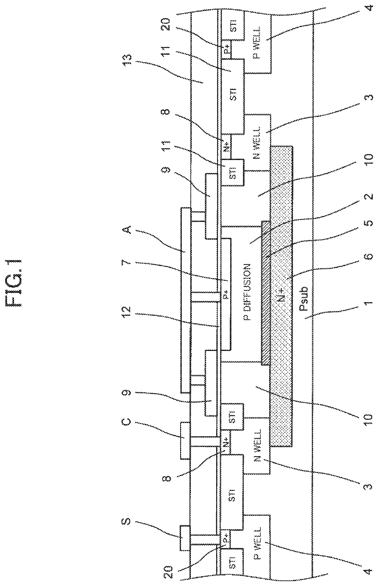
[0050]An avalanche photodiode according to the first embodiment of the present invention will be specifically described with reference to FIG. 1.

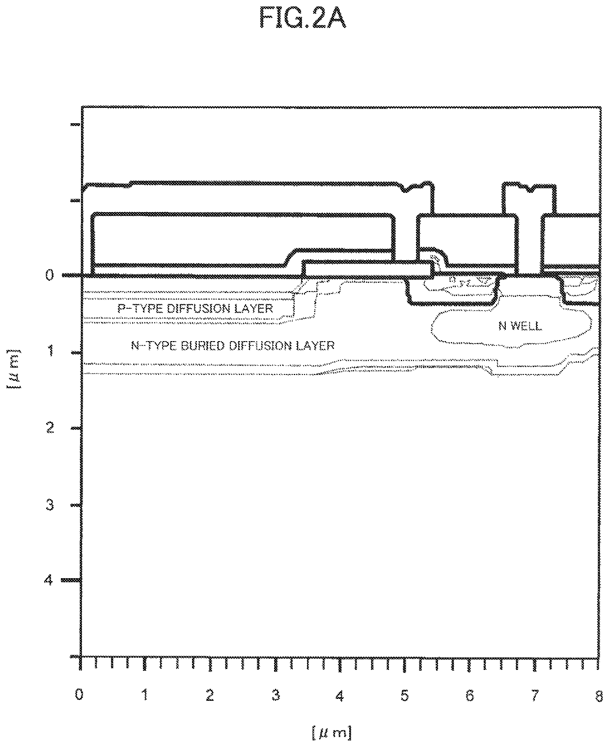
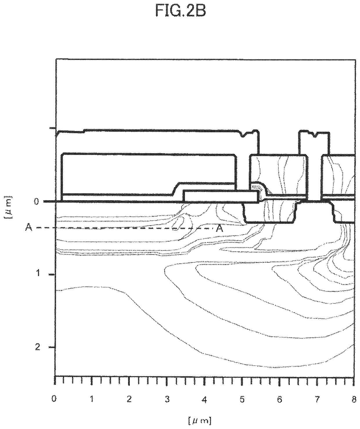
[0051]FIG. 1 is a sectional view of the avalanche photodiode according to the first embodiment of the present invention. In this avalanche photodiode, within a silicon semiconductor substrate 1, which, for example, has a plane orientation of (100) and a resistivity of about 10 Ωcm and is of P type, a low-concentration P-type diffusion layer 2 is formed, which serves as a P-type diffusion layer of an avalanche junction. This low-concentration P-type diffusion layer 2 is formed by ion implantation of boron (11B+). For example, boron (11B+) is implanted under the following three-stage ion implantation conditions.

[0052]

[Ion implantation energy][Dose]200 keV 2.5E+12 cm−250 keV2.5E+12 cm−235 keV1.0E+13 cm−2

[0053]Incidentally, the dose is described with floating-point representation in which an exponential base of 10 is represented by symbol E. Fo...

second embodiment

[0080]An avalanche photodiode according to a second embodiment of the present invention will be described with reference to FIG. 4. The basic configuration is the same as in the first embodiment. This avalanche photodiode according to the second embodiment has the same configuration as in the avalanche photodiode according to the first embodiment except for an N-type buried diffusion layer 25.

[0081]In the avalanche photodiode according to the second embodiment, the N-type buried diffusion layer 25 forming the avalanche junction is formed smaller than, in plan view for the substrate, the bottom portion of the low-concentration P-type diffusion layer 2.

[0082]As in the first embodiment, even when the N-type buried diffusion layer 5 forming the avalanche junction is formed larger than the low-concentration P-type diffusion layer 2, as long as it is substantially not connected to the N-type diffusion layer 3, the potential does not automatically become high, so that the above-described a...

third embodiment

[0085]An avalanche photodiode according to a third embodiment of the present invention will be described with reference to FIG. 5. The basic configuration is the same as in the first embodiment. The difference from the avalanche photodiode according to the first embodiment is another high-concentration N-type buried diffusion layer 35 formed between the N-type diffusion layer 3 serving as the cathode diffusion layer and the N-type buried diffusion layer 6. This N-type buried diffusion layer 35 is an example of the fourth second-conductivity-type semiconductor layer.

[0086]As described in the end of the first embodiment, when the N-type buried diffusion layer 6 is formed at a high ion implantation energy and, as a result, formed at a deep position, the contact concentration between the N-type diffusion layer 3 and the N-type buried diffusion layer 6 becomes low, and the isolation strength between the low-concentration P-type diffusion layer 2 and the P-type semiconductor substrate 1 b...


PUM

PropertyMeasurementUnit
resistivityaaaaaaaaaa
gap widthaaaaaaaaaa
thicknessaaaaaaaaaa

Abstract

An avalanche photodiode includes a first-conductivity-type semiconductor layer; a first second-conductivity-type semiconductor layer; a second second-conductivity-type semiconductor layer; a third second-conductivity-type semiconductor layer; a fourth second-conductivity-type semiconductor layer; a fifth second-conductivity-type semiconductor layer.The first-conductivity-type semiconductor layer and the second second-conductivity-type semiconductor layer form an avalanche junction. The first and third second-conductivity-type semiconductor layers are electrically connected together via the fourth second-conductivity-type semiconductor layer such that the semiconductor substrate and the first-conductivity-type semiconductor layer are electrically isolated from each other.

Description

CROSS REFERENCES TO RELATED APPLICATIONS[0001]This application claims the benefit of priority to Japanese Patent Application No. 2016-192074, filed Sep. 29, 2016, and the entire contents of which are herein incorporated by reference.TECHNICAL FIELD[0002]The present invention relates to an avalanche photodiode, specifically to an avalanche photodiode that has a structure configured to prevent edge breakdown and have a uniform electric-field distribution.BACKGROUND ART[0003]In these years, range-finding sensors have been used for autofocus of cellular phone cameras and for determination of position or distance for automatic robots such as robotic cleaners. In particular, photosensors such as TOF (Time Of Flight) sensors employing avalanche photodiodes operating in Geiger mode have been used because these sensors can determine distance in dark fields and can be provided in reduced sizes.[0004]Avalanche photodiodes are one type of PN diodes used so as to cause avalanche breakdown. In th...

Claims


Application Information

Patent Timeline
Patent Type & Authority Patents(United States)
IPC IPC(8): H01L31/107H01L31/02
CPCH01L31/02027H01L31/107H01L27/14643
Inventor TAKIMOTO, TAKAHIRONATSUAKI, KAZUHIROUCHIDA, MASAYO
Owner SHARP KK
Why Eureka
Try Eureka